background image


LE910Cx HW User Guide


1VV0301298  Rev. 33 

Page 70 of 128 

2021-06-29


Not Subject to NDA 


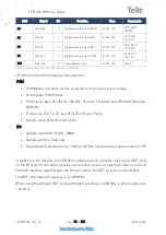
RS232 Pin# 

Signal 

Pad No. 

Name 

Usage 

DTR - DTR_UART 

M14 

Data Terminal 
Ready 

Input to LE910Cx 
that controls the 
DTE READY 
condition 

GND 

A2, B13, D4… 

Ground 

Ground 

DSR - DSR_UART 

P14 

Data Set Ready 

Output from 
LE910Cx that 
indicates that the 
module is ready 

RTS - RTS_UART 

L14 

Request to Send 

Input to LE910Cx 
controlling the 
Hardware flow 
control 

CTS - CTS_UART 

P15 

Clear to Send 

Output from 
LE910Cx controlling 
the Hardware flow 
control 

RI - RI_UART 

R14 

Ring Indicator 

Output from 
LE910Cx indicating 
the Incoming call 
condition 

Table 28: Modem Serial Port 1 Signals 


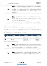
Note: 


DCD, DTR, DSR, RI signals that are not used for UART 

functions can be configured as GPIO using AT commands. 


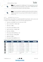
Note: 


To avoid a back-powering effect, it is recommended to prevent 

any HIGH logic level signal from being applied to the module’s digital 
pins when it is powered OFF or during an ON/OFF transition. 


Note: 


For minimum implementations, only the TXD and RXD lines 

need be connected. The other lines can be left open provided a 
software flow control is implemented. 

Summary of Contents for LE910C1-AP

Page 1: ...LE910Cx HW Design Guide 1VV0301298 Rev 33 2021 06 29 Telit Technical Documentation ...

Page 2: ...t LE910C4 NF North America CAT4 variant LE910C1 NF North America CAT1 variant LE910C1 SA North America CAT1 variant AT T LE910C1 SAX North America CAT1 variant AT T LE910C1 ST North America CAT1 variant T Mobile LE910C1 SV North America CAT1 variant Verizon LE910C1 SVX North America CAT1 variant Verizon LE910C1 LA Latin America CAT1 variant LE910C4 LA Latin America CAT4 variant LE910C4 CN China CA...

Page 3: ...Main Features 12 Block Diagram 14 Environmental Requirements 16 2 5 1 Temperature Range 16 2 5 2 RoHS Compliance 16 Operating Frequency Bands 16 2 6 1 RF Bands per Regional Variant 16 2 6 2 Reference Table of RF Bands Characteristics 17 RF Parameters 20 2 7 1 Sensitivity 20 2 7 2 Output power 21 Mechanical Specifications 22 2 8 1 Dimensions 22 2 8 2 Weight 22 3 MODULE CONNECTIONS 23 Pin out 23 Sig...

Page 4: ...ion State 39 Turning off the LE910Cx Module 44 5 3 1 Shutdown by Software Command 44 5 3 2 Hardware Shutdown 45 5 3 3 Unconditional Hardware Shutdown 46 Powering OFF the Module 47 Fast Power Down 47 5 5 1 Fast Shut Down by Hardware 48 5 5 2 Fast Shut Down by Software 50 6 POWER SUPPLY 51 Power Supply Requirements 51 Power Consumption 51 General Design Rules 53 6 3 1 Electrical Design Guidelines 54...

Page 5: ...68 SGMII Interface 68 8 3 1 Ethernet Control interface 68 Serial Ports 69 8 4 1 Modem Serial Port 1 Signals 69 8 4 2 Modem Serial Port 2 71 8 4 3 RS232 Level Translation 72 Peripheral Ports 73 8 5 1 SPI Serial Peripheral Interface 73 8 5 2 I2C Inter integrated Circuit 74 8 5 3 SD MMC Card Interface 75 8 5 4 WiFi SDIO Interface 76 Audio Interface 77 8 6 1 Digital Audio 77 8 6 1 1 Short Frame Timing...

Page 6: ...90 Recommended Footprint for the Application 95 Stencil 97 PCB Pad Design 97 Recommendations for PCB Pad Dimensions mm 97 Solder Paste 98 10 7 1 Solder Reflow 98 10 7 2 Cleaning 99 11 APPLICATION GUIDE 101 Debug of the LE910Cx Module in Production 101 Bypass Capacitor on Power Supplies 101 SIM Interface 102 11 3 1 SIM Schematic Example 102 EMC Recommendations 103 Download and Debug Port 103 11 5 1...

Page 7: ... 117 Copyrights and Other Notices 117 14 1 1 Copyrights 117 14 1 2 Computer Software Copyrights 117 Usage and Disclosure Restrictions 118 14 2 1 License Agreements 118 14 2 2 Copyrighted Materials 118 14 2 3 High Risk Materials 118 14 2 4 Trademarks 118 14 2 5 3rd Party Rights 119 14 2 6 Waiwer of Liability 119 Safety Recommendations 119 15 GLOSSARY 121 16 DOCUMENT HISTORY 122 SECTION 10 X DIMENSI...

Page 8: ...errors to be avoided This document cannot include every hardware solution or every product that can be designed Avoiding invalid solutions must be considered mandatory Where the suggested hardware configurations are not be considered mandatory the information provided should be used as a guide and a starting point for the proper development of the product with the Telit LE910Cx module Note The int...

Page 9: ...r improvements Telit appreciates feedback from the users of on information Symbol Conventions The following conventions are used to emphasize specific types of information Danger This information MUST be followed or catastrophic equipment failure or personal injury may occur Warning Alerts the user on important steps about the module integration Note Tip Provides advice and suggestions that may be...

Page 10: ...Application Note 80000NT11246A Telit_LE920A4_LE910Cx_Wi Fi_Interface_Application_Note_r1 80490NT11511A Antenna Detection Application Note 80000NT10002A High Speed Inter Chip USB Electrical Specification version 1 0 a supplement to the USB 2 0 specification Section 3 8 2 ETH_Expansion_board_Application Note 80490NT11622A LE910C1 LE910C4 PSM Application Note 80502NT11758A ...

Page 11: ...Cx cellular module within user application shall be done according to the design rules described in this manual IT L integrazione del modulo cellulare LE910Cx all interno dell applicazione dell utente dovrà rispettare le indicazioni progettuali descritte in questo manuale DE Die Integration des LE910Cx Mobilfunk Moduls in ein Gerät muß gemäß der in diesem Dokument beschriebenen Kunstruktionsregeln...

Page 12: ...cing Pay as you drive insurance Stolen vehicles tracking Internet connectivity General Functionality and Main Features The LE910Cx series of cellular modules features an LTE and multi RAT modem together with a powerful on chip application processor and a rich set of interfaces The major functions and features are listed below Function Features Modem Multi RAT cellular modem for voice and data comm...

Page 13: ... Processor s file system AT command access High speed WWAN access to external host Diagnostic monitoring and debugging NMEA data to an external host CPU HSIC Optional High speed 480 Mbps 240 MHz DDR USB transfers are 100 host driver compatible with traditional USB cable connected topologies Bidirectional data strobe signal STROBE Bidirectional data signal DATA No power consumption unless a transfe...

Page 14: ...IFI connectivity SD MMC for SD Card connectivity Warning LE910C1 EUX LE910C1 SAX and LE910C1 SVX models which are based on ThreadX OS does not support the following functions Fastboot Wi Fi BT SD MMC HSIC SGMII RNDIS over the USB NMEA over the USB USB Audio USB OTG Audio playback Audio playback during voice call Full duplex voice conversation recording Voice Recording In call music delivery AUX PC...

Page 15: ...r external codec Rich IO interfaces Depending on the LE910Cx software features enabled some of its interfaces exported due to multiplexing may be used internally and therefore may not be usable by the application PMIC with the RTC function inside Figure 1 LE910Cx Block Diagram MEMORIES RF FRONTEND GNSS Antennna GPIO Cellular antenna 1 Cellular antenna 2 PCM In out SIM GNSS_Sync APPLICATION PROCESS...

Page 16: ...is range might slightly deviate from ETSI specifications Storage and non operating temperature range 40 C 90 C Table 3 Temperature Range 2 5 2 RoHS Compliance As a part of the Telit corporate policy of environmental protection the LE910Cx complies with the RoHS Restriction of Hazardous Substances directive of the European Union EU directive 2011 65 EU Operating Frequency Bands The operating freque...

Page 17: ...4 66 LE910C1 SAX 2 4 12 66 LE910C1 ST 2 4 12 66 71 LE910C1 SV 4 13 LE910C1 SVX 4 13 LE910C1 LA 2 3 5 8 1 2 4 5 1 2 3 4 5 7 28 LE910C4 LA 2 3 5 8 1 2 4 5 1 2 3 4 5 7 28 LE910C4 CN 3 8 1 8 1 3 5 8 38 39 40 41M 34 39 LE910C1 WWX 2 3 5 8 1 2 4 5 6 8 19 1 2 3 4 5 7 8 9 12 13 14 18 19 20 25 26 28 LE910C4 WWX 2 3 5 8 1 2 4 5 6 8 19 1 2 3 4 5 7 8 9 12 13 14 18 19 20 25 26 28 Table 4 RF Bands per Regional ...

Page 18: ...784 8 1845 1879 8 Tx 8762 8912 Rx 9237 9387 95 MHz WCDMA 800 B19 830 845 875 890 Tx 312 363 Rx 712 763 45 MHz TDS CDMA 2000 B34 2010 2025 2010 2025 Tx 10054 10121 Rx 10054 10121 0 MHz TDS CDMA 1900 B39 1880 1920 1880 1920 Tx 9404 9596 Rx 9404 9596 0 MHz LTE 2100 B1 1920 1980 2110 2170 Tx 18000 18599 Rx 0 599 190 MHz LTE 1900 B2 1850 1910 1930 1990 Tx 18600 19199 Rx 600 1199 80 MHz LTE 1800 B3 1710...

Page 19: ...500 B21 1447 9 1462 9 1495 9 1510 9 Tx 24450 24599 Rx 6450 6599 48 MHz LTE 1900 B25 1850 1915 1930 1995 Tx 26040 26689 Rx 8040 8689 80 MHz LTE 850 B26 814 849 859 894 Tx 26690 27039 Rx 8690 9039 45 MHz LTE 700 B28A 703 733 758 788 Tx 27210 27510 Rx 9210 9510 55 MHz LTE 700 B28 703 748 758 803 Tx 27210 27659 Rx 9210 9659 55 MHz LTE AWS 3 B66 1710 1780 2210 2200 Tx 131972 132671 Rx 66436 67335 400 M...

Page 20: ...109 5 103 7 WCDMA AWS B4 109 5 110 0 112 106 7 WCDMA 850 B5 110 0 111 0 112 5 104 7 WCDMA 850 B6 110 0 111 0 112 5 106 7 WCDMA 850 B19 110 0 111 0 112 5 106 7 WCDMA 900 B8 109 5 110 5 112 103 7 TDS CDMA 2000 B34 110 0 105 TDS CDMA 1900 B39 110 0 105 LTE 2100 B1 98 0 98 5 100 5 96 3 LTE 1900 B2 97 0 99 0 99 94 3 LTE 1800 B3 97 5 99 5 99 5 93 3 LTE AWS B4 98 0 99 0 100 5 96 3 LTE 850 B5 99 0 100 5 1...

Page 21: ...98 0 97 5 100 5 93 5 LTE TDD 2600 B38 98 0 98 5 100 5 96 3 LTE TDD 1900 B39 98 5 99 5 101 96 3 LTE TDD 2300 B40 97 0 98 5 99 5 96 3 LTE TDD 2500 B41M 97 0 98 0 99 5 94 3 Table 6 sensitivity levels Note The sensitivity level has a deviation about 2dB each model device and channel because the level shows typical value LTE level is measured at BW 10M 2 7 2 Output power Typical values for Max output l...

Page 22: ...15 mm tolerance Thickness 2 2 mm 0 15 mm tolerance and The LE910Cx WWX module s overall dimensions are Length 29 4 mm 0 15 mm tolerance Width 29 4 mm 0 15 mm tolerance Thickness 2 2 mm 0 15 mm tolerance Note LE910C1 SV s thickness is only 2 3mm 0 15 mm tolerance Note Consider a typical label thickness of 0 1 mm in addition to the module thickness 2 8 2 Weight The nominal weight of the LE910Cx modu...

Page 23: ... C107 DSR O Output for Data Set Ready DSR to DTE 1 8V Alternate Fn GPIO_32 M14 C108 DTR I Input for Data Terminal Ready DTR from DTE 1 8V Alternate Fn GPIO_34 N14 C109 DCD O Output for Data Carrier Detect DCD to DTE 1 8V Alternate Fn GPIO_33 R14 C125 RING O Output for Ring Indication RI to DTE 1 8V Alternate Fn GPIO_31 SPI Serial Peripheral Interface AUX UART F15 SPI_CLK O SPI Clock output 1 8V E1...

Page 24: ...i Fi Reset Power enable control 1 8V M11 WLAN_SLEEP_CLK O Wi Fi Sleep clock output 1 8V L4 WOW I Wake On WLAN 1 8V Active Low LTE WiFi Coexistence M8 WCI_TX O Wireless coexistence interface TXD 1 8V M9 WCI_RX I Wireless coexistence interface RXD 1 8V SIM Card Interface 1 A6 SIMCLK1 O External SIM 1 signal Clock 1 8 2 85V A7 SIMRST1 O External SIM 1 signal Reset 1 8 2 85V A5 SIMIO1 I O External SIM...

Page 25: ... Note below General Purpose Digital I O C8 GPIO_01 I O GPIO_01 STAT_LED 1 8V Alternate Fn I2C C9 GPIO_02 I O GPIO_02 1 8V Alternate Fn I2C C10 GPIO_03 I O GPIO_03 1 8V Alternate Fn I2C C11 GPIO_04 I O GPIO_04 1 8V Alternate Fn I2C B14 GPIO_05 I O GPIO_05 1 8V Alternate Fn I2C C12 GPIO_06 I O GPIO_06 1 8V Alternate Fn I2C C13 GPIO_07 I O GPIO_07 1 8V Alternate Fn I2C K15 GPIO_08 I O GPIO_08 SW_RDY ...

Page 26: ...r Input 1 Analog H4 ADC_IN2 AI Analog Digital Converter Input 2 Analog D7 ADC_IN3 AI Analog Digital Converter Input 3 Analog SGMII Interface E4 SGMII_RX_P AI SGMII receive plus PHY F4 SGMII_RX_M AI SGMII receive minus PHY D5 SGMII_TX_P AO SGMII transmit plus PHY D6 SGMII_TX_M AO SGMII transmit minus PHY HSIC Interface A12 HSIC_DATA I O High speed inter chip interface data 1 2V Optional A11 HSIC_ST...

Page 27: ... GND Ground B13 GND Ground D4 GND Ground E1 GND Ground E2 GND Ground E14 GND Ground F2 GND Ground G1 GND Ground G2 GND Ground G7 GND Ground G8 GND Ground G9 GND Ground H1 GND Ground H2 GND Ground H7 GND Ground H8 GND Ground H9 GND Ground J1 GND Ground J2 GND Ground J7 GND Ground J8 GND Ground J9 GND Ground K2 GND Ground L1 GND Ground L2 GND Ground M3 GND Ground M4 GND Ground M12 GND Ground N3 GND ...

Page 28: ...0 GND Ground P13 GND Ground R2 GND Ground R3 GND Ground R5 GND Ground R6 GND Ground R8 GND Ground R10 GND Ground Reserved A8 Reserved Reserved A9 Reserved Reserved A10 Reserved Reserved B2 Reserved Reserved B3 Reserved Reserved B4 Reserved Reserved B5 Reserved Reserved C3 Reserved Reserved C4 Reserved Reserved C5 Reserved Reserved C6 Reserved Reserved C7 Reserved Reserved C14 Reserved Reserved D3 ...

Page 29: ...ved Reserved G3 Reserved Reserved G14 Reserved Reserved H3 Reserved Reserved H15 Reserved Reserved J3 Reserved Reserved J4 Reserved Reserved J14 Reserved Reserved J15 Reserved Reserved K3 Reserved Reserved K4 Reserved Reserved K14 Reserved Reserved L3 Reserved Reserved M5 Reserved Reserved M6 Reserved Reserved M7 Reserved Reserved M10 Reserved Reserved N7 Reserved Reserved N8 Reserved Reserved N10...

Page 30: ... the module side if flow control is not used If the UART port is not used all UART signals can be left disconnected Note Unless otherwise specified RESERVED pins must be left unconnected floating Note The following pins are unique for the LE910Cx and may not be supported on other former or future xE910 family modules Special care must be taken when designing the application board if future compati...

Page 31: ...oint or an USB connector C15 USB_D If not used connect to a Test Point or an USB connector A13 USB_VBUS If not used connect to a Test Point or an USB connector N15 C103 TXD If not used connect to a Test Point M15 C104 RXD If not used connect to a Test Point L14 C105 RTS If flow control is not used connect to GND P15 C106 CTS If not used connect to a Test Point D15 TX_AUX If not used connect to a T...

Page 32: ... new series in the xE910 form factor The LE910Cx is fully backward compatible with the previous xE910 in terms of Mechanical dimensions Package and pin map To support the extra features and additional interfaces the LE910Cx introduces more pins than the xE910 The extra pins of the LE910Cx can be considered as optional if not needed and can be left unconnected floating if not used ...

Page 33: ...1 06 29 Not Subject to NDA In this case the new LE910Cx can be safely mounted on existing carrier boards designed for the previous xE910 The additional pins of the LE910Cx are shown in Figure 3 marked Green Figure 3 LE910Cx vs LE910 Pin out Comparison top view ...

Page 34: ...TRANSIENT Transient voltage on pin VBATT 10 ms 0 5 7 0 V VBATT_PA Battery supply voltage on pin VBATT_PA 0 3 6 0 V Table 9 Absolute Maximum Ratings Not Operational Recommended Operating Conditions Symbol Parameter Min Typ Max Unit Tamb Ambient temperature 40 25 85 C VBATT Battery supply voltage on pin VBATT 3 4 3 8 4 2 V VBATT_PA Battery supply voltage on pin VBATT_PA 3 4 3 8 4 2 V IBATT_PA IBATT ...

Page 35: ...level higher than 2 7V for 1 8V CMOS signals 4 3 1 1 8V Pads Absolute Maximum Ratings Parameter Min Max Input level on any digital pin when on 0 3V 2 16V Input voltage on analog pins when on 0 3V 2 16 V Table 11 Absolute Maximum Ratings Not Functional 4 3 2 1 8V Standard GPIOs Pad Parameter Min Max Unit Comment VIH Input high level 1 25V V VIL Input low level 0 6V V VOH Output high level 1 4V V VO...

Page 36: ...low level 0 0 45V V IIL Low level input leakage current 2 uA No pull up IIH High level input leakage current 2 uA No pull down RPU Pull up resistance 10 100 kΩ RPD Pull down resistance 10 100 kΩ Ci Input capacitance 5 pF Table 13 Operating Range SD Card Pads Working at 1 8V 4 3 4 1 8V SIM Card Pads Pad Parameter Min Max Unit Comment VIH Input high level 1 35V 2V V VIL Input low level 0 3V 0 43V V ...

Page 37: ... Maximum Ratings Not Functional 4 3 6 SD Card Pads 2 95V Pad Parameter Min Max Unit Comments VIH Input high level 1 9V 3 1V V VIL Input low level 0 3V 0 7V V VOH Output high level 2 1V 3 05V V VOL Output low level 0V 0 4V V IIL Low level input leakage current 10 uA No pull up IIH High level input leakage current 10 uA No pull down RPU Pull up resistance 10 100 kΩ RPD Pull down resistance 10 100 kΩ...

Page 38: ...H Output high level 2 25V 3 1V V VOL Output low level 0V 0 4V V IIL Low level input leakage current 10 uA No pull up IIH High level input leakage current 10 uA No pull down RPU Pull up resistance 10 100 kΩ RPD Pull down resistance 10 100 kΩ Ci Input capacitance 5 pF Table 17 Operating Range For SIM Pads Operating at 2 95V ...

Page 39: ...ers should expect to see 800 mV on the output Figure 4 illustrates a simple circuit to power on the module using an inverted buffer output Figure 4 Power on Circuit Note Recommended values R2 47 kΩ R1 10 kΩ Initialization and Activation State After turning on the LE910Cx module a predefined internal boot sequence performs the HW and SW initialization of the module which takes some time to complete...

Page 40: ...to NDA Note During the Initialization state the AT commands are not available The DTE host must wait for the Activation state before communicating with the LE910Cx Figure 5 LE910Cx Initialization and Activation A flow chart showing the proper turn on procedure is displayed below ...

Page 41: ... 06 29 Not Subject to NDA Figure 6 Turn on Procedure Timing of VAUX PWRMON and SW_RDY Models ON VAUX PWRMON ON SW_RDY LE910C1 NA Typ 21 sec Typ 28 Sec LE910C4 NS LE910C1 AP LE910C4 AP LE910C1 EU LE910C4 EU LE910C1 NF LE910C4 NF LE910C1 LA LE910C4 LA LE910C4 CN ...

Page 42: ... completely powered on and is ready to accept AT commands Note During the SW initialization of the LE910Cx the SW configures all pads and interfaces to the desired mode When PWRMON goes high this indicates that the initialization of all I O pads is completed Note Do not use any pull up resistor on the ON_OFF_N line as it is pulled up internally Using a pull up resistor may cause latch up problems ...

Page 43: ... power on sequence immediately after VBATT supply is applied Note Active low signals are labeled with a name that ends with or with _N Note To avoid a back powering effect it is recommended to prevent any HIGH logic level signal from being applied to the module s digital pins when it is powered OFF or during an ON OFF transition Note Waiting time for the AT commands answer can vary between differe...

Page 44: ... shutdown command is sent LE910Cx enters the Finalization state and at the end of the finalization process shuts down PWRMON SW_RDY The duration of the Finalization state may vary according to the current situation of the module so it is not possible to define a value Usually it will take more than 10 seconds from sending a shutdown command until a complete shutdown is achieved The DTE host should...

Page 45: ...r at least 2 5 seconds and then released Use the same circuitry and timing for power on When the ON OFF hold time is above 2 5 seconds the LE910Cx enters the Finalization state and eventually shuts down PWRMON SW_RDY The duration of the Finalization state can differ according to the current module situation so a value cannot be defined Usually it will take more than 15 seconds from sending a shutd...

Page 46: ...he LE910Cx module the HW_SHUTDOWN_N pad must be tied low for at least 200 milliseconds and then released Figure 8 shows a simple circuit for applying an unconditional shutdown Figure 10 Circuit for Unconditional Hardware Shutdown Figure 9 shows the system power down timing when using HW_SHUTDOWN_N Figure 11 Power down timing using HW_SHUTDOWN_N Note Recommended values are as follows R2 47kΩ R1 10k...

Page 47: ...buffers In a complete power supply shut down is needed the below procedure must be followed 1 Perform a HW shutdown as described in Section 5 3 1 2 Wait for the HW Shutdown procedure to complete monitor the PWRMON SW_RDY pin 3 Turn OFF power supply to the module Warning Carefully follow the recommended procedure for shut down and power off Failure to follow the recommended shut down and power off ...

Page 48: ...wishing to implement the Fast Shut Down should configure a GPIO as the trigger pin for the Fast Shut Down through AT command The high to low transition of a GPIO triggers the Fast Shut Down and then the LE910Cx module turns off within 30ms Below is the example hardware configuration for the Fast Shut Down Figure 12 Example for Fast Shut Down circuit Note Consider the voltage drop under max current...

Page 49: ...ow LE910Cx is turned off The following formula can be used to calculate Ctank value to provide the LE910Cx with sufficient energy during the Fast Shut Down The LE910Cx consumes up to 800mA and 30ms is the typical time to perform shutdown and 1V is the minimum voltage margin from the threshold of LE910Cx hardware reset Based on the formula more than 24mF is needed for the Fast Shut Down But the Cta...

Page 50: ...2021 06 29 Not Subject to NDA Warning Ctank associated with low ESR requires current limiting feature in the DCDC converter to avoid inrush current side effects 5 5 2 Fast Shut Down by Software The Fast Power Down can be triggered directly by the AT command ...

Page 51: ...pply 30 mV Table 19 Power Supply Requirements Note For PTCRB approval on the final products the power supply is required to be within the range of the Normal Supply voltage ranger Power Consumption Table 20 provides typical current consumption values of LE910Cx for the various available modes Mode Average Typ Mode Description Switched Off Switched off 10µA Module supplied but switched Off RTC On I...

Page 52: ... Tx 0 dBm 300mA LTE CAT 1 CAT 4 channel BW 20 MHz RB Full RB Tx 0 dBm With FTP TpT session LTE to USB 10Mbps DL 5Mbps UL CAT 1 150Mbps DL 50Mbps UL CAT 4 Operative Mode WCDMA WCDMA Voice 330mA WCDMA voice call Tx 10 dBm WCDMA HSDPA 0 dBm 220mA WCDMA data call Cat 14 Tx 0 dBm Max throughput WCDMA HSDPA 22 dBm 640mA WCDMA data call Cat 14 Tx 22 dBm Max throughput Operative Mode GSM GSM Tx and Rx mod...

Page 53: ...SM GPRS mode the RF transmission is not continuous but is packed into bursts at a base frequency of approximately 216 Hz with relative current peaks up to about 2 0A Therefore the power supply must be designed to withstand these current peaks without large voltage drops This means that both the electrical design and the board layout must be designed for this current flow If the PCB layout is not w...

Page 54: ...erefore a linear regulator can be used A switching power supply is preferred to reduce power consumption When using a linear regulator a proper heat sink must be provided to dissipate the generated power A bypass low ESR capacitor of adequate capacity must be provided to cut the current absorption peaks near the LE910Cx module A 100 μF tantalum capacitor is usually suitable on both VBATT and VBATT...

Page 55: ...e developed as the switching frequency can also generate EMC interference For car batteries lead acid accumulators the input voltage can rise up to 15 8V This must be kept in mind when choosing components all components in the power supply must withstand this voltage A bypass low ESR capacitor of adequate capacity must be provided to cut the current absorption peaks A 100μF tantalum capacitor is u...

Page 56: ...o cut the current absorption peaks a 100μF tantalum capacitor is usually suitable Make sure the low ESR capacitor usually a tantalum one is rated at least 10V A protection diode should be inserted close to the power input to protect the LE910Cx module from power polarity inversion Otherwise the battery connector should be done in a way to avoid polarity inversions when connecting the battery The b...

Page 57: ...r the heat generated by the LE910Cx module consider it to be 2W max during transmission at Class10 GPRS upload In LTE WCDMA HSPA mode the LE910Cx emits RF signals continuously during transmission Therefore special attention must be paid to how to dissipate the heat generated The LE910Cx is designed to conduct heat flow from the module IC s towards the bottom of the PCB across GND metal layers The ...

Page 58: ... drops on the power line at the current peaks frequency of 216 Hz that will reflect on all the components connected to this supply also introducing the noise floor at the burst base frequency For this reason while a voltage drop of 300 400 mV may be acceptable from the RF power loss point of view the same voltage drop may not be acceptable from the noise point of view If the application does not h...

Page 59: ...LE910Cx HW User Guide 1VV0301298 Rev 33 Page 59 of 128 2021 06 29 Not Subject to NDA The power supply input cables must be kept separate from noise sensitive lines such as microphone earphone cables ...

Page 60: ...module family are provided in Section 2 6 1 RF Bands per Regional Variant Gain Gain 3 dBi Impedance 50 Ohm Input power 33 dBm 2 W peak power in GSM 24 dBm average power in WCDMA LTE VSWR absolute max 10 1 limit to avoid permanent damage VSWR recommended 2 1 limit to fulfill all regulatory requirements Table 21 Primary Antenna Requirements Since there is no antenna connector on the LE910Cx module t...

Page 61: ...le since the antenna line loss should be less than around 0 3 dB Line geometry should have uniform characteristics constant cross sections and avoid meanders and abrupt curves Any suitable geometry structure can be used to implement the printed transmission line affecting the antenna If a ground plane is required in the line geometry this plane must be continuous and sufficiently extended so the g...

Page 62: ...ludes an input for a second Rx antenna to improve radio sensitivity The function is called Antenna Diversity Item Value Frequency range The customer must use the most suitable antenna bandwidth to cover the frequency bands provided by the network operator and supported by the OEM while using the Telit module The bands supported by each variant of the LE910Cx module family are provided in Section 2...

Page 63: ...eference_Guide document must be referred to install passive or active GNSS ANT configuration by customer Note If the GNSS is not used connected please disable the GNSS functionality perfectly using the AT GPSP command refer to Ref 1 LE920x4 LE910Cx AT Command User Guide and connect the GNSS pad R9 to a 50 Ohm termination or floating Note The external GNSS pre filter is required for the GLONASS app...

Page 64: ...n Considerations Since there is no antenna connector on the LE910Cx module the antenna must be connected to the LE910Cx through the PCB to the antenna pad If the antenna is not directly connected at the antenna pad of the LE910Cx a PCB line is required This line of transmission must meet the following requirements Item Value Characteristic impedance 50 Ohm Max attenuation 0 3 dB Avoid coupling wit...

Page 65: ...ble Keep the antenna line far away from the LE910Cx power supply lines If there are EM noisy devices such as fast switching ICs around the PCB hosting the LE910Cx ensure shielding the antenna line by burying it inside the layers of PCB and surrounding it with Ground planes or shield it with a metal frame cover If you do not have EM noisy devices around the PCB of LE910Cx use a Micro strip line on ...

Page 66: ...in interface between the LE910Cx module and OEM hardware Interface LE910Cx SGMII For Ethernet support HSIC x1 Optional SD MMC x1 dual voltage interface for supporting SD MMC card SDIO For WIFI support 1 8V only USB USB2 0 OTG support on LE910C1 LA LE910C4 LA and LE910C4 CN SPI Master only up to 50 MHz I2C For sensors audio control UART 2 HS UART up to 4 Mbps Audio I F I2S PCM Analog I O GPIO 10 27...

Page 67: ...terface Signals Note USB_VBUS input power is used internally to detect the USB port and start the enumeration process It is a power supply pin with a maximum consumption of 5 mA Do not use pull up or a voltage divider for sourcing this supply Note Even if USB communication is not used it is still highly recommended to place an optional USB connector on the application board At least USB signal tes...

Page 68: ...lable to the Linux kernel Further details can be found at Ref 8 ETH_Expansion_board_Application Note 8 3 1 Ethernet Control interface When using an external PHY for Ethernet connectivity the LE910Cx also includes the control interface for managing the external PHY Table 27 lists the signals for controlling the external PHY PAD Signal I O Function Type Comment C2 MAC_MDC O MAC to PHY Clock 2 85V Lo...

Page 69: ...at does not need level translation is the 1 8V UART The LE910Cx UART has CMOS levels as described in Section 4 3 Logic Level Specifications 8 4 1 Modem Serial Port 1 Signals On the LE910Cx Serial Port 1 is a 1 8V UART with 7 RS232 signals It differs from the PC RS232 in the signal polarity RS232 is reversed and levels Table 28 lists the signals of LE910Cx Serial Port 1 RS232 Pin Signal Pad No Name...

Page 70: ...o Send Output from LE910Cx controlling the Hardware flow control 9 RI RI_UART R14 Ring Indicator Output from LE910Cx indicating the Incoming call condition Table 28 Modem Serial Port 1 Signals Note DCD DTR DSR RI signals that are not used for UART functions can be configured as GPIO using AT commands Note To avoid a back powering effect it is recommended to prevent any HIGH logic level signal from...

Page 71: ... refer to the application side therefore on the LE910Cx side these signal are in the opposite direction TXD on the application side will be connected to the receive line here named TXD RX_UART of the LE910Cx serial port and vice versa for Rx Note The DTR pin is used to control the UART and system sleep Pulling the DTR pin down prevents the UART and the entire module from entering low power mode DT...

Page 72: ...ere are a multitude of them differing in the number of drivers and receivers and in the levels make sure to get a true RS232 level translator not a RS485 or other standards By convention the driver is the level translator from the 0 1 8V UART to the RS232 level The receiver is the translator from the RS232 level to 0 1 8V UART To translate the whole set of control lines of the UART the following i...

Page 73: ...rt lines are usually connected to a DB9 connector as shown in Figure 14 Signal names and directions are named and defined from the DTE point of view Figure 18 RS232 Serial Port Lines Connection Layout Peripheral Ports In addition to the LE910Cx serial ports the LE910Cx supports the following peripheral ports SPI Serial Peripheral Interface I2C Inter integrated circuit SD MMC Card Interface SDIO In...

Page 74: ...ster output Slave input 1 8V Shared with TX_AUX H14 SPI_CS O SPI chip select output 1 8V Table 30 SPI Signals Figure 19 SPI Signal Connectivity 8 5 2 I2C Inter integrated Circuit The LE910Cx supports an I2C interface on the following pins B11 I2C_SCL B10 I2C_SDA The I2C can also be used externally by the end customer application In addition SW emulated I2C functionality can be used on GPIO pins 1 ...

Page 75: ...rd SD MMC memory cards with the following features Interface with SD MMC memory cards up to 32 GB Max clock 2 95V 50 MHz SDR Max Data 25 MB s SD standard HS SDR25 at 2 95V Max clock 1 8V 200 MHz SDR Max Data 100 MB s SD standard UHS SDR104 at 1 8 V Max clock 1 8V 50 MHz DDR Max Data 50 MB s SD standard UHS DDR50 at 1 8 V Table 31 lists the LE910Cx SD card signals PAD Signal I O Function Type Comme...

Page 76: ...o 50mA so it can only supply the MMC card external pull up resistors The Pull up resistors must be placed on the host application board The card detection input has an internal pull up resistor VMMC can be used to enable the external power supply LDO Enable signal 8 5 4 WiFi SDIO Interface The LE910Cx provides an SDIO port supporting the SDIO3 0 specification which can be used to interface with a ...

Page 77: ...erface_Application_Note_r1 PAD Signal I O Function Type Comments N13 WIFI_SD_CMD O WiFi SD Command 1 8V L13 WIFI_SD_CLK O WiFi SD Clock 1 8V 200 MHz max J13 WIFI_SD_DATA0 I O WiFi SD Serial Data 0 1 8V M13 WIFI_SD_DATA1 I O WiFi SD Serial Data 1 1 8V K13 WIFI_SD_DATA2 I O WiFi SD Serial Data 2 1 8V H13 WIFI_SD_DATA3 I O WiFi SD Serial Data 3 1 8V L12 WIFI_SDRST O WiFi Reset Power enable control 1 ...

Page 78: ... modes using short or long frame sync modes 16 bit linear PCM format PCM clock rates of 128kHz 256 kHz 512 kHz 1024 kHz and 2048 kHz Default 4096kHz Frame size of 8 16 32 64 128 256 bits per frame Sample rates of 8 kHz and 16 kHz I2S Sample rate 8KHz 16KHz 48KHz Sample width is 16bit only Supported I2S standard only Phillips I2S Bus Specifications revised June 5 1996 In addition to the DVI port th...

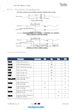
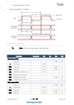
Page 79: ... t syncd PCM_SYNC de asserted time 124 5 µs t clk PCM_CLK cycle time 488 ns t clkh PCM_CLK high time 244 ns t clkl PCM_CLK low time 244 ns t sync_offset PCM_SYNC offset time to PCM_CLK falling 122 ns t sudin PCM_DIN setup time to PCM_CLK falling 60 ns t hdin PCM_DIN hold time after PCM_CLK falling 60 ns t pdout Delay from PCM_CLK rising to PCM_DOUT valid 60 ns t zdout Delay from PCM_CLK falling to...

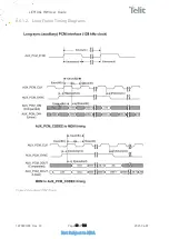
Page 80: ...LE910Cx HW User Guide 1VV0301298 Rev 33 Page 80 of 128 2021 06 29 Not Subject to NDA 8 6 1 2 Long Frame Timing Diagrams Figure 22 Auxiliary PCM Timing ...

Page 81: ...cle time 7 8 µs t auxclkh AUX_PCM_CLK high time 3 8 3 9 µs t auxclkl AUX_PCM_CLK low time 3 8 3 9 µs t suauxsync AUX_PCM_SYNC setup time to AUX_PCM_CLK rising 1 95 ns t hauxsync PCM_DIN hold time after AUX_PCM_CLK rising 1 95 ns t suauxdin AUX_PCM_DIN setup time to AUX_PCM_CLK falling 70 ns t hauxdin AUX_ PCM_DIN hold time after AUX_PCM_CLK falling 20 ns t pauxdout Delay from AUX_PCM_CLK to AUX_PC...

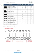
Page 82: ...rnal SCK Frequency 12 288 MHz T Clock period 81 380 ns t HC Clock high 0 45 T 0 55 T ns t LC Clock low 0 45 T 0 55 T ns t sr SD and WS input setup time 16 276 ns t hr SD and WS input hold time 0 ns t dtr SD and WS output delay 65 100 ns t htr SD and WS output hold time 0 ns Using external SCK Frequency 12 288 MHz T Clock period 81 380 ns t HC Clock high 0 45 T 0 55 T ns t LC Clock low 0 45 T 0 55 ...

Page 83: ... can be internally controlled by the LE910Cx firmware and act according to the implementation The following GPIOs are always available as a primary function on the LE910Cx PAD Signal I O Function Type Note C8 GPIO_01 I O Configurable GPIO CMOS 1 8V C9 GPIO_02 I O Configurable GPIO CMOS 1 8V C10 GPIO_03 I O Configurable GPIO CMOS 1 8V C11 GPIO_04 I O Configurable GPIO CMOS 1 8V B14 GPIO_05 I O Conf...

Page 84: ...onfigurable GPIO CMOS 1 8V M9 GPIO_25 I O WCI_RXD Configurable GPIO CMOS 1 8V R14 GPIO_31 I O UART_RI Configurable GPIO CMOS 1 8V P14 GPIO_32 I O UART_DSR Configurable GPIO CMOS 1 8V N14 GPIO_33 I O UART_DCD Configurable GPIO CMOS 1 8V M14 GPIO_34 I O UART_DTR Configurable GPIO CMOS 1 8V F15 GPIO_35 I O SPI_CLK Configurable GPIO CMOS 1 8V E15 GPIO_36 I O SPI_MISO Configurable GPIO CMOS 1 8V D15 GP...

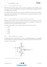
Page 85: ...or with a 10 kΩ pull up resistor to 1 8V 8 7 2 Using a GPIO Pad as an interrupt Wakeup source GPIO pads used as inputs can also be used as an interrupt source for software In general all GPIO pads can also be used as an interrupt However not all GPIO s can be used as a wakeup source of the module wakeup from sleep Only the following GPIO s can be used for waking up the system from sleep GPIO1 GPIO...

Page 86: ...The STAT_LED does not have a dedicated pin The STAT_LED functionality is available on GPIO_01 pin by default GPIO_01 functions as STAT_LED See the AT Command User Guide for details about the AT SLED section LED Status Device Status Permanently off Device off Blinking Blinking 1s on and 2s off Registered in idle Blinking time depends on network condition in order to minimize power consumption Regis...

Page 87: ...e VBATT supply If the battery is removed the RTC is not maintained so if it is necessary to maintain an internal RTC VBATT must be supplied continuously In Power OFF mode the average current consumption is 25uA VAUX Power Output A regulated power supply output is provided to supply small devices from the module This output is active when the module is ON and turns OFF when the module is shut down ...

Page 88: ...ic temperature indications to perform some functions in extreme conditions When properly set see the TEMPMON command in Ref 1 LE920x4 LE910Cx AT Command User Guide it raises a GPIO to High Logic level when the maximum temperature is reached GNSS Characteristics Table 42 specifies the GNSS characteristics and expected performance The values are related to typical environment and conditions Paramete...

Page 89: ...ev 33 Page 89 of 128 2021 06 29 Not Subject to NDA Parameters Typical Measurement Notes Operation limits 515 m sec A GPS Supported Table 42 GNSS Characteristics Note The sensitivity level has a deviation about 2dB each model and device ...

Page 90: ...E910Cx module is designed to be compliant with a standard lead free soldering process Finishing Dimensions The below figure shows the mechanical dimensions of the LE910Cx module Figure 26 LE910Cx Mechanical Dimensions Bottom View except for LE910Cx WWX 3 x Route Inhibit Lead free Alloy Surface finishing Ni Au for all solder pads Pin B1 ...

Page 91: ...ev 33 Page 91 of 128 2021 06 29 Not Subject to NDA Figure 26 1 LE910Cx WWX Mechanical Dimensions Bottom View Note LE910Cx WWX mechanical dimension is bigger than other LE910Cx variants Please refer to 10 3 section for detail information ...

Page 92: ...LE910Cx HW User Guide 1VV0301298 Rev 33 Page 92 of 128 2021 06 29 Not Subject to NDA Figure 27 LE910Cx Mechanical Dimensions Top view with two kinds of shield design except for LE910Cx WWX ...

Page 93: ...0301298 Rev 33 Page 93 of 128 2021 06 29 Not Subject to NDA Figure 28 LE910Cx WWX Mechanical Dimensions Top view Note LE910Cx AP NA NS EU NF ST SA has two sheild design and LE910Cx SV SVX LA CN EUX SAX WWX has one shield design ...

Page 94: ...ser Guide 1VV0301298 Rev 33 Page 94 of 128 2021 06 29 Not Subject to NDA Figure 29 LE910Cx Mechanical Dimensions Side view except for LE910C1 SV and SVX Figure 30 LE910C1 SV and SVX Mechanical Dimensions Side view ...

Page 95: ... it is suggested to design the application board with a 1 5 mm placement inhibit area around the module It is also suggested as a common rule for an SMT component to avoid having a mechanical part of the application board in direct contact with the module Note In the customer application the region marked as INHIBIT WIRING in Figure 31 and 31 1 must be clear of signal wiring or ground polygons Fig...

Page 96: ...6 of 128 2021 06 29 Not Subject to NDA Figure 32 1 Recommended Footprint Top View 181 pads for LE910Cx WWX only Note LE910Cx WWX footprint is same as LE910Cx variants but PCB size is differenct others Please refer to above dimension for LE910Cx WWX ...

Page 97: ...openings can be the same as the recommended footprint 1 1 The suggested thickness of stencil foil is greater than 120 µm PCB Pad Design The solder pads on the PCB are recommended to be of the Non Solder Mask Defined NSMD type Figure 33 PCB Pad Design Recommendations for PCB Pad Dimensions mm Figure 34 PCB Pad Dimensions ...

Page 98: ...mersion Au 3 7 0 05 0 15 Good solder ability protection high shear force values Table 43 Recommendations for PCB Pad Surfaces The PCB must be able to resist the higher temperatures which occur during the lead free process This issue should be discussed with the PCB supplier In general the wettability of tin lead solder paste on the described surface plating is better compared to lead free solder p...

Page 99: ...Temperature max Tsmax Time min to max ts 150 C 200 C 60 180 seconds Tsmax to TL Ramp up rate 3 C second max Time maintained above Temperature TL Time tL 217 C 60 150 seconds Peak temperature Tp 245 0 5 C Time within 5 C of actual peak Temperature tp 10 30 seconds Ramp down rate 6 C second max Time 25 C to peak temperature 8 minutes max Table 44 Solder Profile Characteristics Note All temperatures ...

Page 100: ...ween the module and the host board or even leaks inside the module due to the gap between the module shield and PCB The combination of soldering flux residues and encapsulated solvent could lead to short circuits between conductive parts The solvent could also damage the module label Ultrasonic cleaning could damage the module permanently Especially for crystal oscillators where the risk of damagi...

Page 101: ...onnecting it to an external computer Depending on the customer s application these test pads include but are not limited to the following signals TXD RXD ON OFF HW_SHUTDOWN_N GND VBATT TX_AUX RX_AUX USB_VBUS USB_D USB_D GPIO_09 WCI_RX In addition the following signals are also recommended but not mandatory PWRMON GPIO_01 STAT_LED GPIO_08 SW_RDY Bypass Capacitor on Power Supplies When there is a su...

Page 102: ... bypass capacitor must be mounted on the following lines on the application board VBATT VBATT_PA M1 M2 N1 N2 P1 P2 USB_VBUS Pad A13 Recommended values are 100uF for both VBATT and VBATT_PA together 4 7uF for USB_VBUS including the 1uF capacitor inside the module Customers must still consider that the capacitance mainly depends on the conditions of their application board Generally more capacitance...

Page 103: ...differs according to the specific pin Human body model HBM rating 2000 V JESD22 A114 Charged device model CDM rating 500 V JESD22 C101 Appropriate series resistors must be considered to protect the input lines from overvoltage Download and Debug Port Choose one of the following options in the design of the host system to download or upgrade the Telit software and debug the LE910Cx module when it i...

Page 104: ...by GPIO_09 PAD L15 Asserting this signal high 1 8V during boot will force the system into Fast boot 11 5 2 Recovery Boot Mode Emergency boot download mode is used in case of corrupted boot image has been flashed into the device or in case all other recovery modes failed to work The emergency download mode is triggered by WCI_RX signal PAD M9 Asserting this signal high 1 8V during boot will force t...

Page 105: ...e 105 of 128 2021 06 29 Not Subject to NDA 12 PACKING SYSTEM Packing System Tray The LE910Cx modules are packaged on trays of 36 pieces each as shown in Figure 36 These trays can be used in SMT processes for pick place handling Figure 37 Packing ...

Page 106: ...LE910Cx HW User Guide 1VV0301298 Rev 33 Page 106 of 128 2021 06 29 Not Subject to NDA Figure 38 Tray Drawing ...

Page 107: ...3 Page 107 of 128 2021 06 29 Not Subject to NDA Tape Reel The LE910Cx can be packaged on reels of 200 pieces each See figure for module positioning into the carrier Figure 39 Module Positioning into the Carrier Figure 40 Carrier Tape Detail ...

Page 108: ...LE910Cx HW User Guide 1VV0301298 Rev 33 Page 108 of 128 2021 06 29 Not Subject to NDA Figure 41 Reel Detail Figure 42 Detail Figure 43 Reel Box Detail ...

Page 109: ... Page 109 of 128 2021 06 29 Not Subject to NDA Moisture Sensitivity The LE910Cx module is a Moisture Sensitive Device Level 3 in accordance with standard IPC JEDEC J STD 020 Comply with all the requirements for using this kind of components ...

Page 110: ... or operating in conjunction with any other antenna or transmitter End users and installers must be provided with antenna installation instructions and consider removing the no collocation statement Information on test modes and additional testing requirement The module has been evaluated in mobile stand alone conditions For operational conditions other than a stand alone modular transmitter in a ...

Page 111: ...uvent annuler le droit d utilisation de l appareil par l utilisateur Interference Statement if it is not placed in the device This device complies with Part 15 of the FCC Rules and Industry Canada licence exempt RSS standard s Operation is subject to the following two conditions 1 this device may not cause interference and 2 this device must accept any interference including interference that may ...

Page 112: ...ion de la fréquence de la FCC radiofréquence RF et RSS 102 de la fréquence radio RF ISED règles d exposition Gain de l antenne doit être ci dessous Frequency Band Freq MHz LE910C1 NA Gain dBi LE910C1 NS Gain dBi LE910C1 C4 NF Gain dBi LE910C1 SV Gain dBi LE910C1 C4 LA Gain dBi LE910C1 SA Gain dBi LE910C1 SAX Gain dBi LE910C1 ST Gain dBi 850 MHz 850 3 64 6 08 6 12 NA 3 5 NA NA NA 1900 MHz 1900 2 51...

Page 113: ...ment into an outlet on a circuit different from that to which the receiver is connected Consult the dealer or an experienced radio TV technician for help Labelling Requirements for the Host device The host device shall be properly labelled to identify the modules within the host device The certification label of the module shall be clearly visible at all times when installed in the host device oth...

Page 114: ...En l absence d étiquette l appareil hôte doit porter une étiquette donnant le FCC ID et le IC du module précédé des mots Contient un module d émission du mot Contient ou d une formulation similaire exprimant le même sens comme suit LE910C1 NA Contains FCC ID RI7LE910C1NA Contains IC 5131A LE910C1NA LE910C1 NS Contains FCC ID RI7LE910C1NS Contains IC 5131A LE910C1NS LE910C1 C4 NF Contains FCC ID RI...

Page 115: ... Law are responsible to contact Telit technical support or sales to get the list of these antennas Dial Function The JTBL Module Certification for LE910C1 AP is for non Auto Redial Function device In case customer implement Auto Redial function into Application Device by controlling LE910C1 AP the customer cannot utilize LE910C1 AP JTBL certification and they must apply JTBL as Application Device ...

Page 116: ...ção contra interferência prejudicial e não pode causar interferência em sistemas devidamente autorizados This equipment is not entitled to protection against harmful interference and must not cause interference in duly authorized systems LE910C1 LA Homologation 05818 19 02618 LE910C1 AP Homologation 04679 18 02618 LE910C4 LA Homologation 07669 19 02618 ...

Page 117: ...t products programming or services in your country 14 1 1 Copyrights This instruction manual and the Telit products described herein may include or describe Telit s copyrighted material such as computer programs stored in semiconductor memories or other media Laws in Italy and in other countries reserve to Telit and its licensors certain exclusive rights for copyrighted material including the excl...

Page 118: ...nce with the terms of such agreement 14 2 2 Copyrighted Materials The Software and the documentation are copyrighted materials Making unauthorized copies is prohibited by the law The software or the documentation shall not be reproduced transmitted transcribed even partially nor stored in a retrieval system nor translated into any language or computer language in any form or by any means without p...

Page 119: ...OST OF PROFITS HOWEVER CAUSED AND WHETHER MADE UNDER CONTRACT TORT OR OTHER LEGAL THEORY ARISING IN ANY WAY OUT OF THE USE OR DISTRIBUTION OF THE OTHER CODES OR THE EXERCISE OF ANY RIGHTS GRANTED UNDER EITHER OR BOTH THIS LICENSE AND THE LEGAL TERMS APPLICABLE TO ANY SEPARATE FILES EVEN IF ADVISED OF THE POSSIBILITY OF SUCH DAMAGES 14 2 6 Waiwer of Liability IN NO EVENT WILL TELIT AND ITS AFFILIAT...

Page 120: ...ystem integrator is responsible for the functioning of the final product Therefore the external components of the module as well as any project or installation issue have to be handled with care Any interference may cause the risk of disturbing the GSM network or external devices or having an impact on the security system Should there be any doubt please refer to the technical documentation and th...

Page 121: ...tput GPRS General packet radio services GPS Global positioning system GSM Global system for mobile communications HSIC High speed inter chip I2C Inter integrated circuit LTE Long term evolution RGMII Reduced Gigabit media independent interface SD Secure digital SGMII Serial Gigabit media independent interface SIM Subscriber identity module SMX SmartMX SOC System on Chip SPI Serial peripheral inter...

Page 122: ...d 30 2021 01 29 Section 2 3 Added not supported function only based on TreadX OS models Section 8 5 1 Updated Note 29 2021 01 12 Updated Section 8 6 updated I2S diagram 28 2020 12 08 Updated APPLICABILITY TABLE and added notes Section 3 1 Updated Pin out Section 5 2 Updated Initialization and Activation figure and added timing table Section 5 3 Updated figures Section 14 1 Updated FCC ISED Regulat...

Page 123: ... 5 3 SD MMC Card interface updated 17 2019 10 29 Section 9 1 STATUS LED control updated 16 2019 10 22 Section 2 7 2 Output power updated 15 2019 10 15 Section 3 1 Warning comment removed Table 34 35 note updated Table 18 Updated Idle mode current consumption Section 14 3 Added NCC TW requirement section 14 2019 09 03 Table 18 Updated the current consumption of LTE max power Table 6 Updated the des...

Page 124: ...C1 SV 6 2018 10 25 Table 1 4 Added SA ST SV and LA variants Table 5 Added B14 Section 2 5 1 Updated Temperature Range 5 2018 09 16 Section 14 Adding Antenna gain and FCC ID IC numbers for LE910C1 C4 NF Section 5 2 Fixed typo related to power up timing 4 2018 08 20 Table 1 4 Added LE910C4 EU variant Section 2 3 Updated SIM interface max speed Declared HSIC interface as optional throughout the docum...

Page 125: ...e mode 1 10 2017 12 27 General spelling and grammar edits throughout the document Section 2 3 Updated features list table Section 2 4 Fixed typo in section and inside block diagram 1 09 2017 12 07 Section 14 1 Updated LE910C1 NA 850MHz Max antenna gain Section 6 2 2 Corrected Class12 to Class10 1 08 2017 11 14 Section 2 6 2 Changed B41 to B41M Section 2 7 Renamed from Sensitivity to RF parameters ...

Page 126: ...igure for SHDN_N power down timing Section 8 5 3 Added clarification about VMMC Section 9 7 Added GNSS characteristics 0 6 2016 12 07 Remove all China variant related information 0 5 2016 12 02 Added section 9 2 to better describe SW_RDY signal Minor modifications per typos and improved description Renaming of SHDN_N pin 0 4 2016 11 30 Updated band support table Updated WIFI application note doc i...

Page 127: ...LE910Cx HW User Guide 1VV0301298 Rev 33 Page 127 of 128 2021 06 29 Not Subject to NDA Revision Date Changes 0 2 2016 09 05 Minor edits 0 1 2016 08 30 First Draft ...

Page 128: ......

Reviews: