


Test and Alignment Specification for RT2841 Series (v0.01).docx
Page 8 of 27
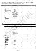
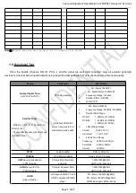
With HDMI 2.0 and
HDCP2.2 player
3820x2160@50&60Hz(4:4:4),HDCP2.2
HDMI3&4 support 4K*2K- Movie
3820x2160@50&60Hz(4:2:0),HDCP2.2
RJ45
(LAN)
DHCP Server
ICMP packets echo request
Headphone
via mini jack adapter
RF signal
Suitable channel
Loud Speakers
/ Enclosures
RF signal
Suitable channel
Audio tones can be defined by the factory (ie: 1KHz & 3KHz, sweep, …).
Picture video formats can be changed by the factory according to their own standard.
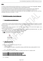
1.6.AD Calibration Test
As the A/D self-calibration mechanism is built-in soc, there’s no any ADC to perform.
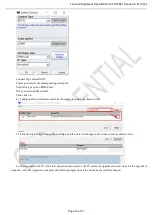
1.7.DDC & EDID & T-Link Test
The E-EDID data structures are according to VESA Enhanced EDID 1.3 (and EIA/CEA-861B for HDMI). CEA Timing
Extension structure has been extended to support all 3D capable timings.
All HDMI structures have their own BIN profile which are part of main SW and uploaded at power-on into soc chipset:
For EDID check, it’s needed to check whether the correct EDID is downloaded by checking corresponding EDID
NVM Checksum or read them out to check bit by bit if it is in line with the released EDID bin file.
1.8.HDCP Test
For HDCP compliancy, it’s needed to check whether the HDCP key has been well set by connecting suitable
generator.
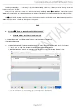
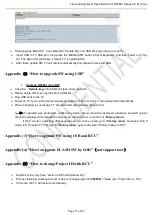
1.9.CI+Key Upgrade, Activation and Test
See Appendix
⑹
“
How to upgrade CI Key using USB
”
See Appendix
⑺
“
How to upgrade Widewine Key using USB
”
See Appendix
⑻
“
How to upgrade PlayReady Key using USB
”(not support at this time)
See Appendix
⑼
“How to upgrade HDCP key key using USB”
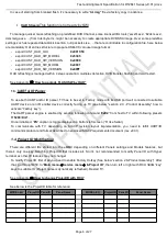
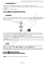
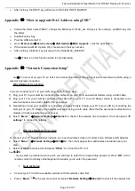
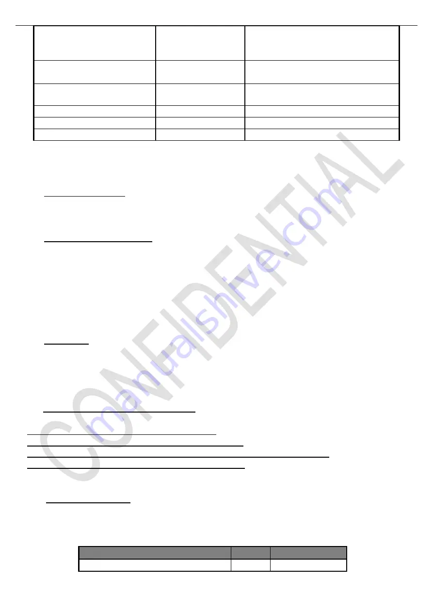
1.10.LAN and WLAN Test
(MAC address and Device/User ID codes)
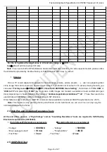
Here are some representative codes examples:
Device ID
User ID
MAC Address
6fa0806936a0ada733262a3f8e8595d5586ce5cb
111382090
00:1C:50:E2:B1:EC
Summary of Contents for RT41VS-EU
Page 32: ...Test and Alignment Specification for RT2841 Series v0 01 docx Page 27 of 27...
Page 33: ...11 Oct 18 Page 8 nRT41 Chassis Block Diagram...
Page 34: ...11 Oct 18 Page 9 nPower supply Block Diagram...
Page 35: ...11 Oct 18 Page 10 nRT41 Power supply Block Diagram...
Page 46: ...11 Oct 18 Page 23 nTrouble Shooting...
Page 47: ...nTrouble Shooting 11 Oct 18 Page 24...
Page 48: ...nTrouble Shooting 11 Oct 18 Page 25...
Page 49: ...11 Oct 18 Page 11 nKey Test Point Main Power Supply 12V 12V Test point...
Page 51: ...11 Oct 18 Page 13 nKey Test Point LDC1 1V5_DDR UDC1 3V3_STB to 1V5_DDR 3V3_STB STR Enable...
Page 52: ...11 Oct 18 Page 14 LDB1 CORE 1V0 nKey Test Point 12V UDDB 12V TO 1V0...
Page 53: ...11 Oct 18 Page 15 LDA1 5V nKey Test Point UDA1 12V TO 5V...
Page 57: ...11 Oct 18 Page 19 nKey Test Point PANEL_VCC 12V Q900 PANEL_VCC...
Page 58: ...11 Oct 18 Page 20 Main Chip 1 SOC Config 2 24MHz CRYSTAL nKey Test Point Test Point...