background image

Chapter 2: Installation

2-13

S-SGPI

O

I-SGPIO

2

BAR CODE

X10DRG-Q

Rev.1.01

MAC CODE

FA

N3

FA

N4

FA

N6/CPU

2

FA

N5/CPU

1

FA

N1

FA

N2

FA

NA

FANB

FANC

FAND

JBT1

LED1

SP1

J2

3

JVR1

JP

AC

1

JVRM

2

JVRM

1

JWD1

JPME

2

JPG1

JPB1

JPL1

JI2C
2

JI2C
1

JTPM

1

JSD1

JSD2

JHD_AC

1

JSPDIF_IN1

JL

1

JITP
1

JPI2C1

JTBT
1

BIOS 

LICENSE

S-SA
TA

0

S-SA
TA

1

I-SA
TA

4

I-SA
TA

5

S-SA
TA

3

S-SA
TA

2

I-SA
TA

1

I-SA
TA

2

I-S

AT

A3

I-SA
TA

0

IPMI CODE

JIPMB1

AUDIO_FP

COM1

JBAT1

JPWR

4

JPWR

2

FA

N-I1

COM2

SUPERDO

M

USB 6 (3.0)

P1-DIMMC

1

P1-DIMMC

2

AL

WA

YS POPULA

TE DIMMx1 FIRST

CPU1

P1-DIMMD

2

P2-DIMME

1

P2-DIMMF

1

P2-DIMME

2

P2-DIMMF

2

LAN2

CPU2

P1-DIMMB

2

P1-DIMMB

1

LAN1

P1-DIMMA

1

P1-DIMMA

2

AL

WA

YS POPULA

TE DIMMx1 FIRST

IPMI_LAN

USB 4/5(3.0)

USB 0/1

P2-DIMMG

1

P2-DIMMH

1

P2-DIMMG

2

AL

WA

YS POPULA

TE DIMMx1 FIRST

P2-DIMMH

2

VGA

CPU2 SLOT

11

 PCI-E 3.0 X8

CPU1 SLOT10 PCI-E 3.0 X8(IN X16)

PCH SLOT9 PCI-E 2.0 X4(IN X8

)

CPU2 SLOT8 PCI-E 3.0 X1

6

CPU2 SLOT6 PCI-E 3.0 X1

6

CPU1 SLOT4 PCI-E 3.0 X1

6

USB 7/8(3.0)

CPU1 SLOT2 PCI-E 3.0 X1

6

USB 2/3

JPWR

3

JPWR

1

JF

1

I-SGPIO

1

P1-DIMMD

1

CLOSE 1st

OPEN 1st

CLOSE 1st

OPEN 1st

LAN

CTRL

BMC

BIOS

PCH

LEDM1

JSTBY1

LED2

Release Tabs

Notches

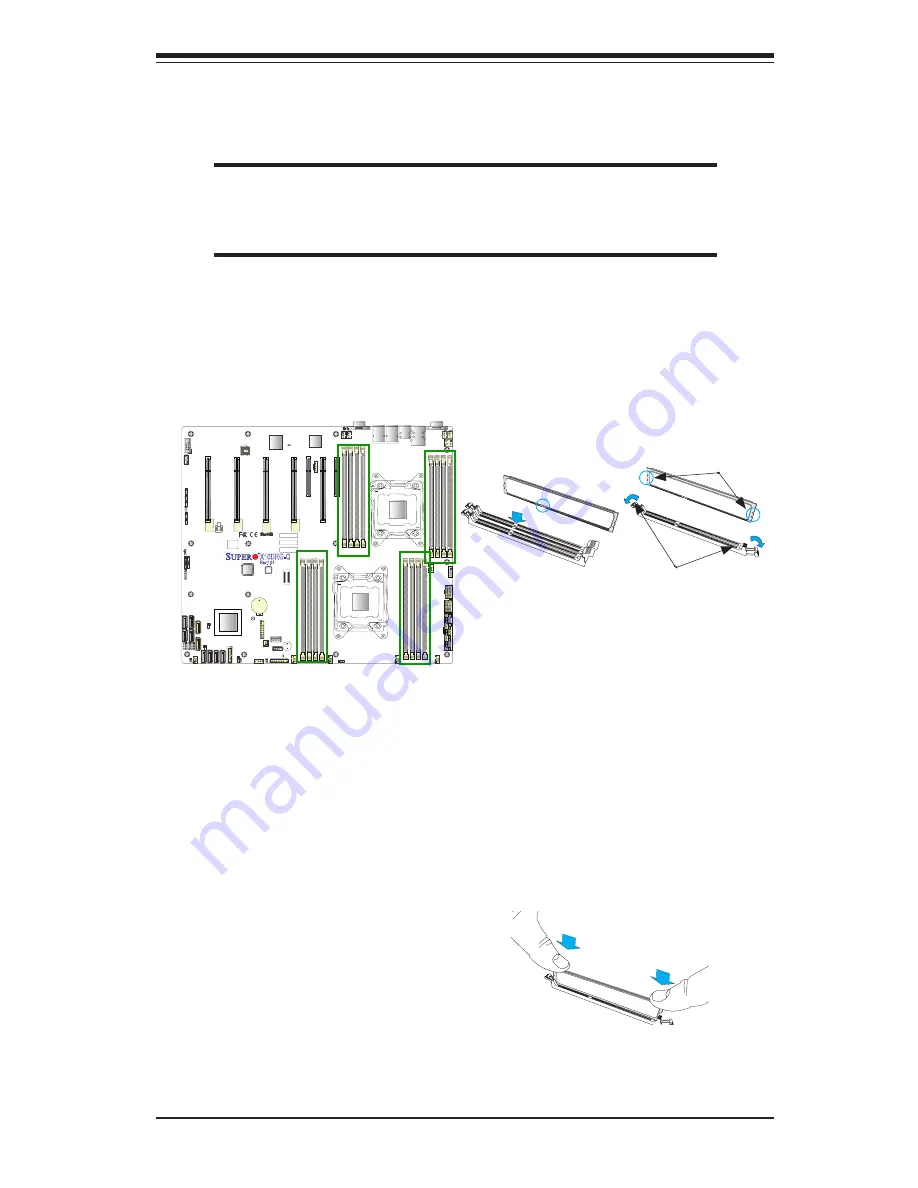
2-5   Installing and Removing the Memory Modules

Note

: Check Supermicro's website for recommended memory modules.

CAUTION


Exercise extreme care when installing or removing DIMM 

modules to prevent any possible damage. 

Installing Memory Modules

1.  Insert the desired number of DIMMs into the memory slots, starting with 

P1-DIMMA1. (For best performance, please use the memory modules of the 
same type and speed in the same bank.)

2.  Push the release tabs outwards on both ends of the DIMM slot to unlock it.

Removing Memory Modules

Press both notches on the ends of the DIMM module to unlock it. Once the DIMM 
module is loosened, remove it from the memory slot.

3.  Align the key of the DIMM module with the receptive point on the memory 

slot.

4.  Align the notches on both ends of the module against the receptive points on 

the ends of the slot.

5.  Use two thumbs together to press the notches on both ends of the module 

straight down into the slot until the module snaps into place.

6.  Press the release tabs to the locking positions to secure the DIMM module 

into the slot.

Press both notches straight 
down into the memory slot at 
the same time.

Summary of Contents for X10DRG-Q

Page 1: ...USER S MANUAL Revision 1 1a X10DRG Q...

Page 2: ...UCH DAMAGES IN PARTICULAR SUPER MICRO COMPUTER INC SHALL NOT HAVE LIABILITY FOR ANY HARDWARE SOFTWARE OR DATA STORED OR USED WITH THE PRODUCT INCLUDING THE COSTS OF REPAIRING REPLACING INTEGRATING INS...

Page 3: ...ting or high end graphics server and workstation platforms Please refer to our website http www supermicro com for CPU and memory support updates Manual Organization Chapter 1 describes the features s...

Page 4: ...installation Warning Important information given to ensure proper system installation or to prevent damage to the components or injury to yourself Note Additional information given to differentiate b...

Page 5: ...Super Micro Computer B V Het Sterrenbeeld 28 5215 ML s Hertogenbosch The Netherlands Tel 31 0 73 6400390 Fax 31 0 73 6416525 Email sales supermicro nl General Information support supermicro nl Technic...

Page 6: ...5 ACPI Features 1 13 1 6 Power Supply 1 13 1 7 Advanced Power Management 1 14 Intel Intelligent Power Node Manager NM Available when the SPM Utility is Installed 1 14 Management Engine ME 1 14 Chapter...

Page 7: ...efinitions 2 22 NMI Button 2 22 Power LED 2 22 HDD UID LED 2 23 NIC1 NIC2 LED Indicators 2 23 Overheat OH Fan Fail UID LED 2 24 Power Fail LED 2 24 Reset Button 2 25 Power Button 2 25 2 7 Connecting C...

Page 8: ...tem Boot Failure 3 2 Losing the System s Setup Configuration 3 2 Memory Errors 3 3 When the System Becomes Unstable 3 3 3 2 Technical Support Procedures 3 5 3 3 Battery Removal and Installation 3 6 Ba...

Page 9: ...Doctor 5 B 2 Appendix C UEFI BIOS Recovery Instructions C 1 An Overview to the UEFI BIOS C 1 C 2 How to Recover the UEFI BIOS Image the Main BIOS Block C 1 C 3 To Recover the Main BIOS Block Using a U...

Page 10: ...X10DRG Q Motherboard User s Manual Notes x...

Page 11: ...t and will not be shipped independently in a retail box No motherboard shipping package will be provided in your shipment Note 1 For your system to work properly please follow the links below to downl...

Page 12: ...therboard Image Note All graphics shown in this manual were based upon the latest PCB Revision available at the time of publishing of the manual The motherboard you ve received may or may not look exa...

Page 13: ...I SATA3 I SATA0 IPMI CODE JIPMB1 AUDIO_FP COM1 JBAT1 JPWR4 JPWR2 FAN I1 COM2 SUPERDOM USB 6 3 0 P1 DIMMC1 P1 DIMMC2 ALWAYS POPULATE DIMMx1 FIRST CPU1 P1 DIMMD2 P2 DIMME1 P2 DIMMF1 P2 DIMME2 P2 DIMMF2...

Page 14: ...2 JHD_AC1 JSPDIF_IN1 JL1 JITP1 JPI2C1 JTBT1 BIOS LICENSE S SATA0 S SATA1 I SATA4 I SATA5 S SATA3 S SATA2 I SATA1 I SATA2 I SATA3 I SATA0 IPMI CODE JIPMB1 AUDIO_FP COM1 JBAT1 JPWR4 JPWR2 FAN I1 COM2 SU...

Page 15: ...k panel COM Port 1 Serial Port 2 for front access FAN 1 2 3 4 5 6 FAN A B C D CPU system cooling fan headers Fans 1 6 Fans A D Fan 5 CPU Fan1 Fan 6 CPU Fan2 JF1 Front_Panel_Control header JIPMB1 4 pin...

Page 16: ...3 0 ports 4 5 FP USB 2 3 2 0 USB 2 0 connections 2 3 header for front access FP USB 6 3 0 Type A USB 3 0 connector 6 for front access FP USB 7 8 3 0 USB 3 0 connections 7 8 header for front access VG...

Page 17: ...board DIMM sizes DIMM Up to 64GB at 1 2V Chipset Intel PCH C612 Expansion Four 4 PCI E 3 0 x16 slots Slot2 Slot4 supported by CPU1 Slot6 Slot8 supported by CPU2 One 1 PCI E 2 0 x4 in x8 slot with TBT...

Page 18: ...SB 2 0 header for two USB 2 0 front accessible connections USB 2 3 One 1 USB 3 0 header for two USB 3 0 front accessible connections USB 7 8 One 1 USB 3 0 Type A header front access USB 6 Thunderbolt...

Page 19: ...ge 3 1V Memory voltage 1 2V Chipset voltage 1 05V CPU 6 Phase switching voltage regulator CPU System overheat LED and control CPU Thermal Trip support Status Monitor for speed control Status Monitor f...

Page 20: ...DR4 DIMM DDR4 DIMM BMC SATA Gen 3 REAR AST2400 DDR4 DIMM B DDR4 DIMM C D SocketID 01 E H F 1 2 1 2 1 1 1 2 1 2 x16 Slot6 JPCIE6 SocketID 00 PCH SPI SPI FLASH 16MB BIOS SPI FLASH 16MB BMC DDR3 VGA IPMI...

Page 21: ...2nm Processing Technology the X10DRG Q dramatically increases performance for a multitude of server applica tions The PCH C612 chip provides Enterprise SMbus and MCTP support with the fol lowing featu...

Page 22: ...nt to the screen The user can adjust the voltage thresholds to define the sensitivity of the voltage monitor Fan Status Monitor with Firmware Control The system health monitoring support provided by t...

Page 23: ...oard accommodates ATX 24 pin 12V 8 pin and 12V 4 pin power connectors Although most power supplies generally meet the specifications required by the CPU some are inadequate In addition two 8 pin power...

Page 24: ...wer management for maximum energy efficiency Although IPNM Specification Version 2 0 3 0 is supported by the BMC Baseboard Management Controller your system must also have IPNM compatible Manage ment...

Page 25: ...omponents Read this section in its entirety before installing or configuring components in the Supermicro chassis Battery Handling Warnung Bei Einsetzen einer falschen Batterie besteht Explosionsgefah...

Page 26: ...xplosi n si la bater a se reemplaza de manera incorrecta Re emplazar la bater a exclusivamente con el mismo tipo o el equivalente recomen dado por el fabricante Desechar las bater as gastadas seg n la...

Page 27: ...dieses Produkts sollte gem allen Bestimmungen und Gesetzen des Landes erfolgen Advertencia Al deshacerse por completo de este producto debe seguir todas las leyes y regla mentos nacionales Attention L...

Page 28: ...not touch its components periph eral chips memory modules or gold contacts When handling chips or modules avoid touching their pins Put the motherboard and peripherals back into their antistatic bags...

Page 29: ...PWR3 JPWR1 JF1 I SGPIO1 P1 DIMMD1 CLOSE 1st OPEN 1st CLOSE 1st OPEN 1st LAN CTRL BMC BIOS PCH LEDM1 JSTBY1 LED2 2 3 Motherboard Installation All motherboards have standard mounting holes to fit differ...

Page 30: ...the chassis as needed 5 Install the motherboard into the chassis carefully to avoid damaging mother board components 6 Using the Phillips screwdriver insert a Pan head 6 screw into a mounting hole on...

Page 31: ...chassis before you install the CPU heatsink When receiving a motherboard without a processor pre installed make sure that the plastic CPU socket cap is in place and none of the socket pins are bent o...

Page 32: ...Close 1st fully retracted gently push down on the lever labelled Open 1st to open the load plate Lift the load plate to open it completely 1 2 Press down on Load Lever Close 1st 1 Pull lever away from...

Page 33: ...not drop the CPU on the socket Do not move the CPU horizontally or vertically Do not rub the CPU against the surface or against any pins of the socket to avoid damaging the CPU or the socket Warning...

Page 34: ...e the load plate with the CPU inside the socket Lock the lever labelled Close 1st first then lock the lever labelled Open 1st second Using your thumb gently push the load levers down to the lever lock...

Page 35: ...ket underneath 3 Screw in two diagonal screws i e the 1 and the 2 screws until just snug do not over tighten the screws to avoid possible damage to the CPU 4 Finish the installation by fully tightenin...

Page 36: ...eatsink to loosen it from the CPU Do not use excessive force when wriggling the heatsink 3 Once the CPU is loosened from the socket remove the CPU from the CPU socket 4 Remove the used thermal grease...

Page 37: ...CLOSE 1st OPEN 1st LAN CTRL BMC BIOS PCH LEDM1 JSTBY1 LED2 Release Tabs Notches 2 5 Installing and Removing the Memory Modules Note Check Supermicro s website for recommended memory modules CAUTION E...

Page 38: ...Optimal Performance Number of CPUs DIMMs CPU and Memory Population Configuration Table For memory to work properly please follow the instructions below 1 CPU 2 DIMMs CPU1 P1 DIMMA1 P1 DIMMB1 1 CPU 4 D...

Page 39: ...LRDIMM and RDIMM ECC Memory Modules An Important Note For the memory modules to work properly please install DIMM modules of the same type and speed on the motherboard Mixing of DIMMs of different ty...

Page 40: ...B 6 3 0 P1 DIMMC1 P1 DIMMC2 ALWAYS POPULATE DIMMx1 FIRST CPU1 P1 DIMMD2 P2 DIMME1 P2 DIMMF1 P2 DIMME2 P2 DIMMF2 LAN2 CPU2 P1 DIMMB2 P1 DIMMB1 LAN1 P1 DIMMA1 P1 DIMMA2 ALWAYS POPULATE DIMMx1 FIRST IPMI...

Page 41: ...2 0 X4 IN X8 CPU2 SLOT8 PCI E 3 0 X16 CPU2 SLOT6 PCI E 3 0 X16 CPU1 SLOT4 PCI E 3 0 X16 USB 7 8 3 0 CPU1 SLOT2 PCI E 3 0 X16 USB 2 3 JPWR3 JPWR1 JF1 I SGPIO1 P1 DIMMD1 CLOSE 1st OPEN 1st CLOSE 1st OP...

Page 42: ...B 2 3 JPWR3 JPWR1 JF1 I SGPIO1 P1 DIMMD1 CLOSE 1st OPEN 1st CLOSE 1st OPEN 1st LAN CTRL BMC BIOS PCH LEDM1 JSTBY1 LED2 1 Backpanel USB 4 USB3 0 2 Backpanel USB 5 USB3 0 3 FP USB 7 8 USB 3 0 4 Type A U...

Page 43: ...MMA1 P1 DIMMA2 ALWAYS POPULATE DIMMx1 FIRST IPMI_LAN USB 4 5 3 0 USB 0 1 P2 DIMMG1 P2 DIMMH1 P2 DIMMG2 ALWAYS POPULATE DIMMx1 FIRST P2 DIMMH2 VGA CPU2 SLOT11 PCI E 3 0 X8 CPU1 SLOT10 PCI E 3 0 X8 IN X...

Page 44: ...IRST IPMI_LAN USB 4 5 3 0 USB 0 1 P2 DIMMG1 P2 DIMMH1 P2 DIMMG2 ALWAYS POPULATE DIMMx1 FIRST P2 DIMMH2 VGA CPU2 SLOT11 PCI E 3 0 X8 CPU1 SLOT10 PCI E 3 0 X8 IN X16 PCH SLOT9 PCI E 2 0 X4 IN X8 CPU2 SL...

Page 45: ...LOT11 PCI E 3 0 X8 CPU1 SLOT10 PCI E 3 0 X8 IN X16 PCH SLOT9 PCI E 2 0 X4 IN X8 CPU2 SLOT8 PCI E 3 0 X16 CPU2 SLOT6 PCI E 3 0 X16 CPU1 SLOT4 PCI E 3 0 X16 USB 7 8 3 0 CPU1 SLOT2 PCI E 3 0 X16 USB 2 3...

Page 46: ...ivity LED Power LED The Power LED connection is located on pins 15 and 16 of JF1 Refer to the table on the right for pin definitions NMI Button The non maskable interrupt button header is located on p...

Page 47: ...and 12 of JF1 and for LAN Port 2 is on pins 9 and 10 Attach the NIC LED cables here to display network activity Refer to the table on the right for pin definitions HDD UID LED The HDD LED connection i...

Page 48: ...Red LED on pin 8 provides warnings of overheating fan failure or power failure The Blue LED on pin 7 works as the front panel UID LED indicator Refer to the tables on the right for pin definitions OH...

Page 49: ...ht for pin definitions Power Button Pin Definitions JF1 Pin Definition 1 Signal 2 Ground Reset Button The Reset Button connection is located on pins 3 and 4 of JF1 Attach it to a hardware reset switch...

Page 50: ...7 Connecting Cables Power Connectors A 24 pin ATX main power supply con nector JPWR1 two 8 pin CPU power connectors JPWR2 JPWR3 and a 4 pin connector JPWR4 are located on the motherboard These power c...

Page 51: ...VGA CPU2 SLOT11 PCI E 3 0 X8 CPU1 SLOT10 PCI E 3 0 X8 IN X16 PCH SLOT9 PCI E 2 0 X4 IN X8 CPU2 SLOT8 PCI E 3 0 X16 CPU2 SLOT6 PCI E 3 0 X16 CPU1 SLOT4 PCI E 3 0 X16 USB 7 8 3 0 CPU1 SLOT2 PCI E 3 0 X...

Page 52: ...U2 SLOT8 PCI E 3 0 X16 CPU2 SLOT6 PCI E 3 0 X16 CPU1 SLOT4 PCI E 3 0 X16 USB 7 8 3 0 CPU1 SLOT2 PCI E 3 0 X16 USB 2 3 JPWR3 JPWR1 JF1 I SGPIO1 P1 DIMMD1 CLOSE 1st OPEN 1st CLOSE 1st OPEN 1st LAN CTRL...

Page 53: ...LOT8 PCI E 3 0 X16 CPU2 SLOT6 PCI E 3 0 X16 CPU1 SLOT4 PCI E 3 0 X16 USB 7 8 3 0 CPU1 SLOT2 PCI E 3 0 X16 USB 2 3 JPWR3 JPWR1 JF1 I SGPIO1 P1 DIMMD1 CLOSE 1st OPEN 1st CLOSE 1st OPEN 1st LAN CTRL BMC...

Page 54: ...U1 SLOT10 PCI E 3 0 X8 IN X16 PCH SLOT9 PCI E 2 0 X4 IN X8 CPU2 SLOT8 PCI E 3 0 X16 CPU2 SLOT6 PCI E 3 0 X16 CPU1 SLOT4 PCI E 3 0 X16 USB 7 8 3 0 CPU1 SLOT2 PCI E 3 0 X16 USB 2 3 JPWR3 JPWR1 JF1 I SGP...

Page 55: ...3 0 P1 DIMMC1 P1 DIMMC2 ALWAYS POPULATE DIMMx1 FIRST CPU1 P1 DIMMD2 P2 DIMME1 P2 DIMMF1 P2 DIMME2 P2 DIMMF2 LAN2 CPU2 P1 DIMMB2 P1 DIMMB1 LAN1 P1 DIMMA1 P1 DIMMA2 ALWAYS POPULATE DIMMx1 FIRST IPMI_LA...

Page 56: ...LOT10 PCI E 3 0 X8 IN X16 PCH SLOT9 PCI E 2 0 X4 IN X8 CPU2 SLOT8 PCI E 3 0 X16 CPU2 SLOT6 PCI E 3 0 X16 CPU1 SLOT4 PCI E 3 0 X16 USB 7 8 3 0 CPU1 SLOT2 PCI E 3 0 X16 USB 2 3 JPWR3 JPWR1 JF1 I SGPIO1...

Page 57: ...E 2 0 X4 IN X8 CPU2 SLOT8 PCI E 3 0 X16 CPU2 SLOT6 PCI E 3 0 X16 CPU1 SLOT4 PCI E 3 0 X16 USB 7 8 3 0 CPU1 SLOT2 PCI E 3 0 X16 USB 2 3 JPWR3 JPWR1 JF1 I SGPIO1 P1 DIMMD1 CLOSE 1st OPEN 1st CLOSE 1st...

Page 58: ...E 3 0 X16 CPU1 SLOT4 PCI E 3 0 X16 USB 7 8 3 0 CPU1 SLOT2 PCI E 3 0 X16 USB 2 3 JPWR3 JPWR1 JF1 I SGPIO1 P1 DIMMD1 CLOSE 1st OPEN 1st CLOSE 1st OPEN 1st LAN CTRL BMC BIOS PCH LEDM1 JSTBY1 LED2 CMOS Cl...

Page 59: ...1 FIRST P2 DIMMH2 VGA CPU2 SLOT11 PCI E 3 0 X8 CPU1 SLOT10 PCI E 3 0 X8 IN X16 PCH SLOT9 PCI E 2 0 X4 IN X8 CPU2 SLOT8 PCI E 3 0 X16 CPU2 SLOT6 PCI E 3 0 X16 CPU1 SLOT4 PCI E 3 0 X16 USB 7 8 3 0 CPU1...

Page 60: ...PCI E 3 0 X8 IN X16 PCH SLOT9 PCI E 2 0 X4 IN X8 CPU2 SLOT8 PCI E 3 0 X16 CPU2 SLOT6 PCI E 3 0 X16 CPU1 SLOT4 PCI E 3 0 X16 USB 7 8 3 0 CPU1 SLOT2 PCI E 3 0 X16 USB 2 3 JPWR3 JPWR1 JF1 I SGPIO1 P1 DIM...

Page 61: ...X8 IN X16 PCH SLOT9 PCI E 2 0 X4 IN X8 CPU2 SLOT8 PCI E 3 0 X16 CPU2 SLOT6 PCI E 3 0 X16 CPU1 SLOT4 PCI E 3 0 X16 USB 7 8 3 0 CPU1 SLOT2 PCI E 3 0 X16 USB 2 3 JPWR3 JPWR1 JF1 I SGPIO1 P1 DIMMD1 CLOSE...

Page 62: ...t CLOSE 1st OPEN 1st LAN CTRL BMC BIOS PCH LEDM1 JSTBY1 LED2 LAN Link Indicator LED Settings LED Color Definition Off No Connection 10 Mbps Green 100 Mbps Amber 1 Gbps 2 9 Onboard LED Indicators A LAN...

Page 63: ...9 PCI E 2 0 X4 IN X8 CPU2 SLOT8 PCI E 3 0 X16 CPU2 SLOT6 PCI E 3 0 X16 CPU1 SLOT4 PCI E 3 0 X16 USB 7 8 3 0 CPU1 SLOT2 PCI E 3 0 X16 USB 2 3 JPWR3 JPWR1 JF1 I SGPIO1 P1 DIMMD1 CLOSE 1st OPEN 1st CLOSE...

Page 64: ...IMMG2 ALWAYS POPULATE DIMMx1 FIRST P2 DIMMH2 VGA CPU2 SLOT11 PCI E 3 0 X8 CPU1 SLOT10 PCI E 3 0 X8 IN X16 PCH SLOT9 PCI E 2 0 X4 IN X8 CPU2 SLOT8 PCI E 3 0 X16 CPU2 SLOT6 PCI E 3 0 X16 CPU1 SLOT4 PCI...

Page 65: ...the motherboard and chassis 2 Disconnect all ribbon wire cables from the motherboard including those for the keyboard and mouse 3 Remove all add on cards 4 Install CPU 1 first making sure it is fully...

Page 66: ...unplugging the power cord and contracting both pads on the CMOS Clear Jumper JBT1 Refer to Section 2 8 in Chapter 2 2 Remove all components from the motherboard especially the DIMM modules Make sure t...

Page 67: ...ted in their slots Follow the instructions given in Section 2 5 in Chapter 2 6 Please follow the instructions given in the DIMM Population Tables listed in Section 2 5 to install your memory modules W...

Page 68: ...ng properly 3 Using minimum configuration for troubleshooting Remove all unnecessary components starting with add on cards first and use minimum configuration with a CPU and a memory module installed...

Page 69: ...s chapter or see the FAQs on our website http www supermicro com before contacting Technical Support 2 BIOS upgrades can be downloaded from our website http www supermicro com 3 If you still cannot re...

Page 70: ...y with the regulations set up by your local hazardous waste management agency to dispose of your used battery properly 3 3 Battery Removal and Installation Battery Removal To remove the onboard batter...

Page 71: ...re downloading You can choose from the zip file and the exe file If you choose the zip BIOS file please unzip the BIOS file onto a bootable USB device Run the batch file using the format FLASH bat fil...

Page 72: ...ntly displayed on the outside of the shipping carton and the shipping package is mailed prepaid or hand carried Shipping and handling charges will be applied for all orders that must be mailed when se...

Page 73: ...splays all the options that can be configured Grayed out options cannot be configured Options in blue can be configured by the user The right frame displays the key legend Above the key legend is an a...

Page 74: ...om the main menu you can access the other setup screens An AMI BIOS identification string is displayed at the left bottom corner of the screen below the copyright message Warning Do not upgrade the BI...

Page 75: ...displays the system time in HH MM SS format e g 15 32 52 Supermicro X10DRG Q BIOS Version This item displays the version of the BIOS ROM used in this system Build Date This item displays the date that...

Page 76: ...of the normal POST messages The options are Enabled and Disabled AddOn ROM Display Mode This item sets the display mode for the Option ROM Select Keep Current to use the current AddOn ROM Display set...

Page 77: ...main memory can be saved in a non volatile memory area such as in a hard drive and then power down the system Enable S5 to power off the whole system except the power supply unit PSU and keep the pow...

Page 78: ...ssor Minimum Ratio Microcode Revision L1 Cache RAM L2 Cache RAM L3 Cache RAM CPU1 Version CPU2 Version Clock Spread Spectrum Select Enable to enable Clock Spectrum support which will allow the BIOS to...

Page 79: ...r 64 bytes if this feature is set to Disabled The CPU prefetches both cache lines for 128 bytes as comprised if this feature is set to Enabled DCU Streamer Prefetcher Available when supported by the C...

Page 80: ...tings The options are Disable Energy Efficiency and Custom If the above is set to Custom the following options are displayed CPU P State Control EIST P States EIST Enhanced Intel SpeedStep Technology...

Page 81: ...ons are Enabled and Disabled Enhanced Halt State C1E Select Enabled to use Enhanced Halt State technology which will significantly reduce the CPU s power consumption by reducing the CPU s clock cycle...

Page 82: ...GT s Gen 2 Generation 2 5 GT s and Gen 3 Generation 3 8 GT s IIO2 Configuration II02 Port 1A Link Speed Select GEN1 to enable PCI Exp Generation 1 support for Port 1A Select GEN2 to enable PCI Exp Gen...

Page 83: ...other transactions that have already been enqueued The options are Disable and Enable Intel VT for Directed I O VT d Intel VT for Directed I O VT d Select Enable to use Intel Virtualization Technology...

Page 84: ...in cloud computing The options are Enable Disable and Auto Early Snoop Available when the OS and the CPU support this feature Select Enabled for Early Snoop support to enhance system performance The...

Page 85: ...e the 4G Address space to be split between two sockets The options are Enable and Disable A7 Mode Select Enabled to support the A7 Addressing mode to improve memory per formance The options are Enable...

Page 86: ...rmed Use the keyboard to enter a value from 0 24 The Default setting is 24 Demand Scrub Demand Scrubbing is a process that allows the CPU to correct correctable memory errors found on a memory module...

Page 87: ...d USB 3 0 Support Select Enabled for USB 3 0 support The options are Smart Auto Auto Enabled Disabled and Manual EHCI1 Select Enabled to enable EHCI Enhanced Host Controller Interface support on USB 2...

Page 88: ...lect AHCI to configure a SATA drive specified by the user as an AHCI drive Select RAID to configure a SATA drive specified by the user as a RAID drive The options are IDE AHCI and RAID If the item abo...

Page 89: ...led present or not Port 0 Port 5 SATA Device Type Available when a SATA port is detected Use this item to specify if the SATA port specified by the user should be con nected to a Solid State drive or...

Page 90: ...pecify if the SATA port specified by the user should be con nected to a Solid State drive or a Hard Disk Drive The options are Hard Disk Drive and Solid State Drive sSATA Configuration When this subme...

Page 91: ...ng down the system The options are Enabled and Disabled sSATA Port 0 Port 3 Spin Up Device On an edge detect from 0 to 1 set this item to allow the PCH to start a COMRE SET initialization to the devic...

Page 92: ...oller sSATA Controller and Both sSATA Port 0 Port 1 This item displays the information detected on the installed sSATA drives on the particular sSATA port Model number of drive and capacity Software P...

Page 93: ...evice to generate a PERR SERR number for a PCI Bus Signal Error Event The options are Enabled and Disabled Above 4G Decoding Available if the system supports 64 bit PCI decoding Select Enabled to deco...

Page 94: ...Use this item to select the high memory size according to memory address mapping for the IO hub The options are 256G 128G 512G and 1024G CPU1 SLOT2 PCI E 3 0 x16 OPRPM CPU1 SLOT4 PCI E 3 0 x16 OPRPM C...

Page 95: ...and the Interrupt Request address of a serial port specified by the user Change Port 1 Settings Change Port 2 Settings This feature specifies the base I O port address and the Interrupt Request addres...

Page 96: ...and VT UTF8 Bits Per second Use this item to set the transmission speed for a serial port used in Console Redirection Make sure that the same speed is used in the host computer and the client computer...

Page 97: ...yed on a terminal and send it as text messages to a remote server The options are Disabled and Enabled Resolution 100x31 Select Enabled for extended terminal resolution support The options are Dis abl...

Page 98: ...used in Console Redirection Make sure that the same speed is used in the host computer and the client computer A lower transmission speed may be required for long and busy lines The options are 9600 1...

Page 99: ...Use this feature to select the number of rows and columns used in Console Redirection for legacy OS support The options are 80x24 and 80x25 Putty KeyPad This feature selects Function Keys and KeyPad s...

Page 100: ...when the receiving buffer is empty The options are None Hardware RTS CTS and Software Xon Xoff The setting for each these features is displayed Data Bits Parity Stop Bits ACPI Settings WHEA Support S...

Page 101: ...From Thunderbolt Devices This feature allows a Thunderbolt device to wake up the system The options are Enabled and Disabled AIC Support This item allows you to apply the Go2Sx command before a Thunde...

Page 102: ...abled and Disabled Thunderbolt SwSMI Delay Use this feature to configure the Thunderbolt Software SMI Delay Enter a numeric value in milliseconds Default is 0 TBT Device IO resource Support This featu...

Page 103: ...o support Runtime Error Logging The options are Enabled and Disabled If this item is set to Enable the following item will be available for con figuration Erasing Settings Erase Event Log Select Enabl...

Page 104: ...is 1 METW Multiple Event Count Time Window This item is used to determine how long in minutes should the multiple event counter wait before generating a new event log Enter a number between 0 to 99 T...

Page 105: ...our system System Event Log Enabling Disabling Options SEL Components Select Enabled to enable all system event logging support at bootup The options are Enabled and Disabled Erasing Settings Erase SE...

Page 106: ...item above Update IPMI LAN Configuration is set to Yes Use this item to select the IP address source for this computer If Static is selected you will need to know the IP address of this computer and e...

Page 107: ...the BIOS setup without sav ing click Yes to quit BIOS without saving the changes or click No to quit the BIOS and save changes 4 6 Security Settings This menu allows the user to configure the followin...

Page 108: ...sed for system boot The options are Legacy UEFI and Dual Fixed Boot Order Priorities This option prioritizes the order of bootable devices from which the system will boot Press Enter on each entry fro...

Page 109: ...ual Boot Order 14 Dual Boot Order 15 Boot Option File Path Create After the driver option name and the file path are set press Enter to enter to submenu and click OK to create the new boot option driv...

Page 110: ...Reset When you have completed the system configuration changes select this option to leave the BIOS setup utility and reboot the computer for the new system configura tion parameters can take effect S...

Page 111: ...gs designed for maximum system performance but not for maximum stability Save As User Defaults To set this feature select Save as User Defaults from the Exit menu and press En ter This enables the use...

Page 112: ...4 40 X10DRG Q Motherboard User s Manual Notes...

Page 113: ...are usually communicated through a series of audible beeps The numbers on the fatal error list correspond to the number of beeps for the cor responding error A 1 BIOS Error Beep Codes Motherboard BIOS...

Page 114: ...A 2 X10DRG Q Motherboard User s Manual Notes...

Page 115: ...you may down load individual drivers and utilities After creating a CD DVD with the ISO files insert the disk into the CD DVD drive on your system and the display shown below should appear Note 1 Clic...

Page 116: ...mes in local and remote management versions and can be used with Nagios to maximize your system monitoring needs With SuperDoctor 5 Man agement Server SSM Server you can remotely control power on off...

Page 117: ...off control to a computer system at bootup C 2 How to Recover the UEFI BIOS Image the Main BIOS Block A UEFI BIOS flash chip consists of a recovery BIOS block and a main BIOS block a main BIOS image...

Page 118: ...f a USB device or a writeable CD DVD Note If you cannot locate the Super ROM file in your driver disk visit our website at www supermicro com to download the BIOS image into a USB flash device and ren...

Page 119: ...want to start with BIOS recovery If you decide to proceed with BIOS recovery follow the procedures below 5 When the screen as shown above displays using the arrow key select the item Proceed with flas...

Page 120: ...ng the message that BIOS update is completed unplug the AC power cable from the power supply to clear the CMOS and then plug the AC power cable in the power supply again to power on the system 10 Pres...

Page 121: ...risis recovery flash that will update the main BIOS block An on call BIOS boot block corruption may occur due to a software tool issue see the image below or an unexpected power outage during BIOS upd...

Page 122: ...Jumper JBR1 1 Power down the system 2 Close pins 2 3 on Jumper JBR1 and power on the system 3 Follow the BIOS recovery SOP listed in the previous chapter Appendix C 4 After completing the steps above...

Page 123: ...expected to result in significant injury or loss of life or catastrophic property damage Accordingly Supermicro disclaims any and all liability and should buyer use or sell such products for use in su...

Reviews: