background image

Chapter 2: Installation

2-11

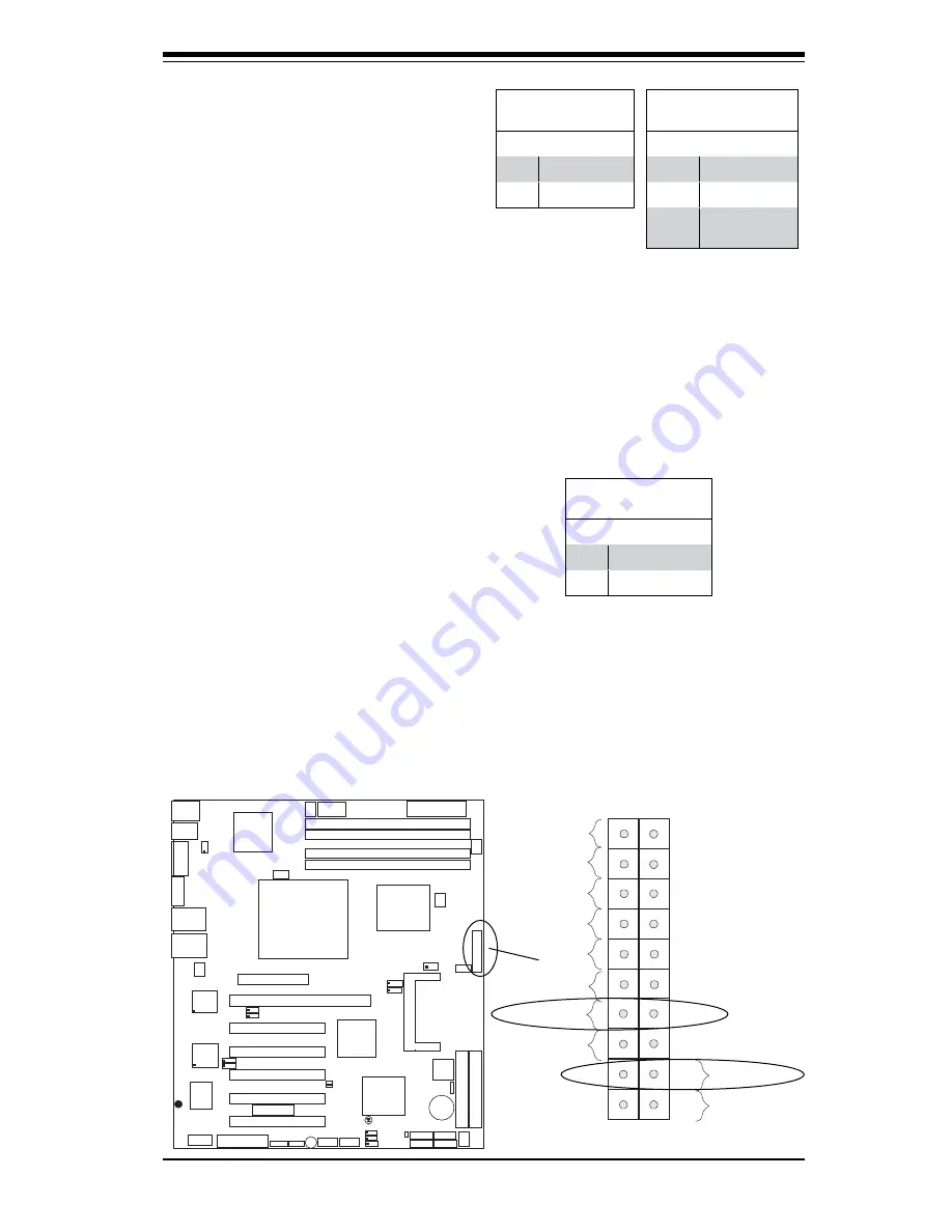
Power Button

OH/Fan Fail LED

1

NIC1 LED

Reset Button

2

HDD LED

Power LED

Reset

PWR

Vcc

Vcc

Vcc

Vcc

Ground

Ground

19

20

Vcc

X

Ground

NMI

X

Vcc

X

NIC2 LED

OH/Fan Fail  LED

Overheat/FanFail LED

Connect an LED cable to the OH/Fan 

Fail  connection  on  pins  7  and  8  of 

JF1  to  provide  advanced  warnings 

of  chassis  overheating  or  system  fan 

failure.  Refer to the table on the right 

for pin defi nitions.  

Reset

OH/Fan Fail LED

Pin Defi nitions (JF1)

Pin#     Defi nition     

7

Vcc

8

Ground

OH/Fan Fail Indicator 

Status

State     Defi nition     

Off

Normal

On

Overheat

Flash-
ing

Fan Fail

Reset Button 

The  Reset  Button  connection  is  lo-

cated on pins 3 and 4 of JF1.  Attach 

it to the hardware reset switch on the 

computer case.  Refer to the table on 

the right for pin defi nitions.  

Reset Button

Pin Defi nitions (JF1)

Pin#     Defi nition     

3

Reset

4

Ground

PCI 32-bit 33 MHz

S

U

P

E

R


 P

D

S

M

A

®

  CPU

LGA 775

KB/MS

C

O

M

1

JLAN1

E7230

North  Bridge

J P L 1

J L1

J L E D

24-Pin ATX PWR

ICH7R

J

F

1

South  Bridge

J31

J28

8-pin PWR

Battery

J 9

F

P

 C

T

R

L

USB 1/2

J15

V

G

A

JG1

JLAN2

LAN1

CTRL

S I/O

Printer

J P L 2

Floppy

Slot1

DIMM 2B

PCI-X 133 MHz

BIOS

PXH-V

Mukilteo

JPW1

J 27

P

ri

m

a

ry


ID

E

J

4

J

3

JWOR

L

E

1

JBT1

USB3/4

USB5/6

J P 3

JPF

J W D

WOL

Fan3

DIMM 1B

DIMM 2A

DIMM 1A

DIMM 1

DIMM 2

DIMM 3

DIMM 4

JPW2

VGA

CTRL

Slot6

L E 3

L E 4

*C

o

m

p

a

c

F

la

s

h


o

n

ly

COM2

Slot2

Slot3

Slot4

Slot5

PCI 32-bit 33 MHz

JI2C1

JI2C2

J

P

G

1

LAN2

CTRL

IP

M

2

.0

SATA0
SATA1

SATA2

SATA3

J 46

J 45

F

a

n

1

F

a

n

4

Fan6

F

a

n

2

F

a

n

5

PCI 32-bit 33 MHz

PCI 32-bit 33 MHz

PCI 32-bit 33 MHz

JW

F

1

P

W

3

SPKR

Slot7

PCI-Exp.  x8

Summary of Contents for Supero PDSMA

Page 1: ...PDSMA USER S MANUAL Revision 1 0d...

Page 2: ...RDWARE SOFTWARE OR DATA Any disputes arising between manufacturer and customer shall be governed by the laws of Santa Clara County in the State of California USA The State of California County of Sant...

Page 3: ...by a technician Manual Organization Chapter 1 describes the features specifications and performance of the PDSMA mainboard and provides detailed information about the chipset Chapter 2 provides hardwa...

Page 4: ...Features 1 8 1 3 PC Health Monitoring 1 10 1 4 Power Configuration Settings 1 10 1 5 ACPI Features 1 11 1 6 Power Supply 1 11 Chapter 2 Installation 2 1 Static Sensitive Devices 2 1 2 2 Processor and...

Page 5: ...nnector 2 18 2 7 Jumper Settings 2 19 Explanation of Jumpers 2 19 GLAN Enable Disable 2 19 CMOS Clear 2 20 VGA Enable 2 20 Watch Dog Enable 2 21 SMBus to PCI PCI Exp Slots 2 21 Power Force On Enable D...

Page 6: ...ed Questions 3 3 3 4 Returning Merchandise for Service 3 4 Chapter 4 BIOS 4 1 Introduction 4 1 4 2 Running Setup 4 2 4 3 Main BIOS Setup 4 2 4 4 Advanced Setup 4 7 4 5 Security Setup 4 19 4 6 Boot Set...

Page 7: ...standards in quality and performance Please check that the following items have all been included with your motherboard If anything listed here is damaged or missing contact your retailer All items a...

Page 8: ...perMicro Computer B V Het Sterrenbeeld 28 5215 ML s Hertogenbosch The Netherlands Tel 31 0 73 6400390 Fax 31 0 73 6416525 Email sales supermicro nl General Information support supermicro nl Technical...

Page 9: ...nt Note to the User All images and layouts shown in this manual were based upon the latest PCB Revision available at the time of publishing of this manual The motherboard you ve received may or may no...

Page 10: ...ted with a Compact Flash Card J3 the blue slot will be available for one device only if not J3 can be used for multiple devices Figure 1 3 Motherboard Layout not drawn to scale PCI 32 bit 33 MHz S UPE...

Page 11: ...ector Pins 3 4 Internal Buzzer Pins 1 4 External Speaker Cable JL1 Chassis Intrusion Header JLED Power LED JWF1 Compact Flash Card PWR Connector Note 2 KB MS J28 PS 2 Keyboard Mouse Connector Printer...

Page 12: ...HT feature in the BIOS under Advanced Setting before install ing a supported OS Note visit www Intel com for CPU support and driver updates OS Licensing Support Intel Dual Core CPU supports Windows 20...

Page 13: ...Onboard I O 1 ATA 100 EIDE Channel Intel ICH7R SATA Controller 4 connectors for 4 devices with support of RAID functions 0 1 5 and 10 1 floppy port interface up to 2 88 MB 1 Fast UART 16550 compatible...

Page 14: ...ard MUKILTEO E7230 LGA775_PROCESSOR ICH 7R USB PORT_0 7 MS KB FDD SER 1 SER 2 PRN VRM 10 1 ADDR CTRL CTRL ADDR DATA DATA UDMA 100 VRM V10 1 DMI S ATA 3Gb 4 x SATA CK410 CLK MCH PORTS FSB 1066 800 533M...

Page 15: ...nterface arbitration re quired for the system to operate efficiently It also provides the bandwidth needed for the system to maintain its peak performance The Direct Media Interface DMI provides the c...

Page 16: ...llows the user to define an overheat temperature When this temperature reaches the threshold the CPU thermal trip feature will be activated and it will send a signal to the Speaker LED and at the same...

Page 17: ...as WOL capability Note that Wake On LAN can only be used with an ATX 2 01 or above compliant power supply 1 5 ACPI Features ACPI stands for Advanced Configuration and Power Interface The ACPI specific...

Page 18: ...eets ATX power supply Specification 2 02 or above Also your power supply must supply 1 5A for the Ethernet ports It must also be SSI compliant info at http www ssiforum org Additionally in areas where...

Page 19: ...re removing the board from the antistatic bag Handle the board by its edges only do not touch its components peripheral chips memory modules or gold contacts When handling chips or modules avoid touch...

Page 20: ...U heatsink 2 Intel s boxed Pentium 4 CPU package contains the CPU fan and heatsink as sembly If you buy a CPU separately make sure that you use only Intel certified multi directional heat sinks and fa...

Page 21: ...ligned carefully lower the CPU straight down to the socket Do not drop the CPU on the socket Do not move the CPU horizontally or vertically Do not rub the CPU against the surface or against any pins o...

Page 22: ...if the protective film is not removed from the heatsink 5 Apply the proper amount of thermal grease on the CPU Note if your heatsink came with a thermal pad please skip this step 6 If necessary rearra...

Page 23: ...nents when installing the motherboard into the chassis 8 Repeat Step 6 to insert all four heatsink fasteners into the mounting holes 9 Once all four fasteners are securely inserted into the mounting h...

Page 24: ...u may populate any number of DIMM slots Populating DIMM 1A DIMM 1B and or DIMM 2A DIMM 2B with modules of the same size and of the same type will result in dual channel two way interleaved memory whic...

Page 25: ...s and LED indicators Refer to the follow ing section for descriptions and pin definitions Figure 2 4 JF1 Header Pins VGA Blue Green Mouse Green Power Button OH Fan Fail LED 1 NIC1 LED Reset Button 2 H...

Page 26: ...power supply connector JPW1 on the PDSMA meets the SSI Superset ATX specification You can only use a 24 pin power supply cable on the motherboard Make sure that the ori entation of the connector is co...

Page 27: ...Pin Definitions JF1 Pin Definition 19 Control 20 Ground PCI 32 bit 33 MHz S UPER PDSMA CPU LGA 775 KB MS COM1 JLAN1 E7230 North Bridge JPL1 JL1 JLED 24 Pin ATX PWR ICH7R J F 1 South Bridge J31 J28 8...

Page 28: ...z JWF1 PW3 SPKR Slot7 PCI Exp x8 HDD LED The HDD LED connection is located on pins 13 and 14 of JF1 Attach the hard drive LED cable here to display disk activities including Serial ATA and IDE drive a...

Page 29: ...JF1 Attach it to the hardware reset switch on the computer case Refer to the table on the right for pin definitions Reset Button Pin Definitions JF1 Pin Definition 3 Reset 4 Ground PCI 32 bit 33 MHz S...

Page 30: ...J9 FP CTRL USB1 2 J15 VGA JG1 JLAN2 LAN1 CTRL SI O Printer JPL2 Floppy Slot1 DIMM 2B PCI X133MHz BIOS PXH V Mukilteo JPW1 J27 Primary IDE J 4 J 3 JWOR LE1 JBT1 USB3 4 USB5 6 JP3 JPF JWD WOL Fan3 DIMM...

Page 31: ...I 2 0 SATA0 SATA1 SATA2 SATA3 J46 J45 Fan1 Fan4 Fan6 Fan2 Fan5 PCI32 bit33MHz PCI32 bit33MHz PCI32 bit33MHz JWF1 PW3 SPKR Slot7 PCI Exp x8 Chassis Intrusion A Chassis Intrusion header is located at JL...

Page 32: ...A3 J46 J45 Fan1 Fan4 Fan6 Fan2 Fan5 PCI32 bit33MHz PCI32 bit33MHz PCI32 bit33MHz JWF1 PW3 SPKR Slot7 PCI Exp x8 USB 1 2 FP USB5 6 Universal Serial Bus USB There are two Universal Serial Bus ports USB...

Page 33: ...an1 Fan4 Fan6 Fan2 Fan5 PCI32 bit33MHz PCI32 bit33MHz PCI32 bit33MHz JWF1 PW3 SPKR Slot7 PCI Exp x8 ATX PS 2 Keyboard and PS 2 Mouse Ports The ATX PS 2 keyboard and PS 2 mouse are located next to the...

Page 34: ...Hz PCI32 bit33MHz PCI32 bit33MHz JWF1 PW3 SPKR Slot7 PCI Exp x8 Fan 2 Fan 5 Fan Header Pin Definitions Fan1 6 Pin Definition 1 Ground Black 2 12V Red 3 Tachometer 4 PWM_Control Fan Headers The PDSMA h...

Page 35: ...Fan2 Fan5 PCI32 bit33MHz PCI32 bit33MHz PCI32 bit33MHz JWF1 PW3 SPKR Slot7 PCI Exp x8 Wake On Ring The Wake On Ring header is located at JWOR on the motherboard This function allows your computer to...

Page 36: ...JWD WOL Fan3 DIMM 1B DIMM 2A DIMM 1A DIMM 1 DIMM 2 DIMM 3 DIMM 4 JPW2 VGA CTRL Slot6 L E 3 L E 4 Compact Flash only COM2 Slot2 Slot3 Slot4 Slot5 PCI32 bit33MHz JI2C1 JI2C2 JPG1 LAN2 CTRL IPMI 2 0 SATA...

Page 37: ...n6 Fan2 Fan5 PCI32 bit33MHz PCI32 bit33MHz PCI32 bit33MHz JWF1 PW3 SPKR Slot7 PCI Exp x8 2 7 Jumper Settings Explanation of Jumpers To modify the operation of the motherboard jumpers can be used to ch...

Page 38: ...I32 bit33MHz PCI32 bit33MHz JWF1 PW3 SPKR Slot7 PCI Exp x8 CMOS Clear JBT1 is used to clear CMOS Instead of pins this jumper consists of contact pads to prevent the accidental clearing of CMOS To clea...

Page 39: ...bit33MHz PCI32 bit33MHz JWF1 PW3 SPKR Slot7 PCI Exp x8 Watch Dog Enable JWD controls Watch Dog a system monitor that takes action when a soft ware application freezes the system Closing Pins 1 2 will...

Page 40: ...1 PW3 SPKR Slot7 PCI Exp x8 Power Force On Enable Disable Jumper JPF allows you to enable or disable the Power Force On function If enabled the power will always stay on automatically If this function...

Page 41: ...Slot7 PCI Exp x8 LAN1 Port GLAN LEDs There are two GLAN ports on the mother board Each Gigabit Ethernet LAN port has two LEDs The yellow LED indicates activity while the other LED may be green amber...

Page 42: ...connecting the floppy and hard disk drive cables The floppy disk drive cable has seven twisted wires A red mark on a wire typically designates the location of pin 1 A single floppy disk drive ribbon c...

Page 43: ...r J4 is reserved for Compact Flash Card use only See the note below See the table on the right pin definitions Note J4 the white slot is reserved for Compact Flash Card only Do not use it for other de...

Page 44: ...sh only COM2 Slot2 Slot3 Slot4 Slot5 PCI32 bit33MHz JI2C1 JI2C2 JPG1 LAN2 CTRL IPMI 2 0 SATA0 SATA1 SATA2 SATA3 J46 J45 Fan1 Fan4 Fan6 Fan2 Fan5 PCI32 bit33MHz PCI32 bit33MHz PCI32 bit33MHz JWF1 PW3 S...

Page 45: ...nstall a CPU and heatsink Be sure that it is fully seated and then connect the chassis speaker and the power LED to the motherboard Check all jumper settings as well No Power 1 Make sure that there ar...

Page 46: ...till supplies 3VDC If it does not replace it with a new one 3 If the above steps do not fix the Setup Configuration problem contact your vendor for repairs 4 Make sure to use the correct type of CMOS...

Page 47: ...on Why does Microsoft Windows XP SP2 and Windows Vista show less memory than what is physically installed Answer Microsoft implemented a design change in Windows XP with Service Pack 2 SP2 and Windows...

Page 48: ...IDE cable that came with your system has two connectors to support two drives This special cable must be used to take advantage of the speed the ATA100 66 technology offers Connect the blue connector...

Page 49: ...lays etc in the CMOS The CMOS memory requires very little electrical power When the computer is turned off a backup battery provides power to the BIOS flash chip enabling it to retain system parameter...

Page 50: ...shown below appears briefly at the bottom of the screen during the POST Power On Self Test press the Delete key to activate the main Setup menu Press the Delete key to enter Setup Note Please load Sys...

Page 51: ...arrow keys highlight the month day and year fields and enter the correct data Press the Enter key to save the data BIOS Date This feature allows the BIOS to display the date when the this version of B...

Page 52: ...Controller Mode is set to Enhanced the following items will display Serial ATA SATA RAID Select Enable to enable the function of Serial ATA RAID The options are Enabled and Disabled Default For the Wi...

Page 53: ...options of these items Set the correct configurations accordingly The items included in the sub menu are Type This option allows the user to selects the type of IDE hard drive The option Auto will al...

Page 54: ...lock to be used in multi sector transfer The options are Disabled 4 Sectors 8 Sectors and 16 Sectors LBA Mode Control This item determines if the BIOS will access the Primary IDE Master Device via the...

Page 55: ...ptions are described in this section uBoot Features Access the submenu to make changes to the following settings Quick Boot Mode If enabled this feature will speed up the POST Power On Self Test routi...

Page 56: ...odem Ring Select On to wake your system up when an incoming call is received by your modem The options are On and Off Resume On PME Select On to control the System Wake Up features from the PME of a P...

Page 57: ...the same time Select Write Protect to prevent data from being written into the base memory area of Block 0 512K Select Write Back to allow the CPU to write data back directly from the buffer without w...

Page 58: ...the submenu to make changes to the following settings for PCI devices Onboard G Lan1 2 OPROM Configuration Enabling this option provides the capability to boot from GLAN The options are Disabled and...

Page 59: ...ging the Advanced settings Incorrect values entered may cause system malfunction Also a very high DRAM frequency or incorrect DRAM timing may cause system instability When this occurs revert to the de...

Page 60: ...stems Machine Checking Available when supported by the CPU Set to Enabled to activate the function of Machine Checking and allow the CPU to detect and report hardware machine errors via a set of model...

Page 61: ...tiple operating systems and applications in independent partitions creating multiple virtual systems in one physical computer The options are Enabled and Disabled Note If there is any change to this s...

Page 62: ...B The options are Normal IR Infra Red and ASK IR Base I O Address This setting allows you to select the base I O address for Serial Port B The options are 3F8 2F8 3E8 and 2E8 Interrupt This setting a...

Page 63: ...es to the following settings Event Log Validity This is a display to inform you of the event log validity It is not a setting Event Log Capacity This is a display to inform you of the event log capaci...

Page 64: ...ing is 60 seconds OS Boot Timeout This item sets the amount time allowed for the OS to boot the system before a system reset Key in a number between 0 seconds to 255 seconds The default setting is 60...

Page 65: ...19 2K 38 4K 57 6K and 115 2K Console Type This item allows you to set console redirection type The options are VT100 VT100 8bit PC ANSI 7bit PC ANSI VT100 VT UTF8 and ASCII Flow Control This item all...

Page 66: ...ature increases the fan speed will also increase and vice versa If the option is set to 3 pin fan the fan speed is controlled by voltage If the option is set to 4 pin the fan speed will be controlled...

Page 67: ...supervisor password has been entered User Password Is This feature indicates if a user password has been entered to the system Clear means such a password has not been used and Set means a user passwo...

Page 68: ...following display Highlighting a setting with a or will expand or collapse that entry See details on how to change the order and specs of boot devices in the Item Specific Help window All Boot BIOS s...

Page 69: ...Discarding Changes Highlight this item and hit Enter to exit the BIOS Setup utility without saving any changes you may have made Load Setup Defaults Highlight this item and hit Enter to load the defau...

Page 70: ...4 22 PDSMA User s Manual Notes...

Page 71: ...z PCI32 bit33MHz JWF1 PW3 SPKR Slot7 PCI Exp x8 Appendix A BIOS POST Messages and LED Indicators During the Power On Self Test POST the BIOS will check for problems If a prob lem is found the BIOS wil...

Page 72: ...ror was de tected System RAM Failed at offset nnnn System RAM failed at offset nnnn of in the 64k block at which the error was de tected Extended RAM Failed at offset nnnn Extended memory notworking o...

Page 73: ...rror is cleared the next time the system is booted Memory Size found by POST differed from CMOS Memory size found by POST differed from CMOS Diskette drive A error Diskette drive B error Drive A or B...

Page 74: ...for the specified device CD ROM Drive CD ROM Drive identified Entering SETUP Starting Setup program Failing Bits nnnn The hex number nnnn is a map of the bits at the RAM address which failed the memor...

Page 75: ...e screen If it cannot locate the address it displays Parity is a method for checking errors in binary data A parity error indicates that some data has been corrupted Parity Check 2 nnnn Parity error f...

Page 76: ...dow RAM UMB upper limit segment address nnnn Displays the address nnnn of the upper limit of Upper Memory Blocks indicating released segments of the BIOS which can be reclaimed by a virtual memory man...

Page 77: ...ttempt to initialize video and write the error in the top left corner of the screen The following is a list of codes that may be written to port 80h Appendix B BIOS POST Codes POST Code Description 02...

Page 78: ...system BIOS ROM 3Ah Auto size cache 3Ch Advanced configuration of chipset registers 3Dh Load alternate registers with CMOS values 41h Initialize extended memory for RomPilot 42h Initialize interrupt...

Page 79: ...80h Disable onboard Super I O ports and IRQs 81h Late POST device initialization 82h Detect and install external RS232 ports 83h Configure non MCD IDE controllers 84h Detect and install external para...

Page 80: ...tBoot optional B6h Check password optional B7h Initialize ACPI BIOS B9h Prepare Boot BAh Initialize SMBIOS BBh Initialize PnP Option ROMs BCh Clear parity checkers BDh Display MultiBoot menu BEh Clear...

Page 81: ...Eh Shadow Boot Block EFh System memory test F0h Initialize interrupt vectors F1h Initialize Run Time Clock F2h Initialize video F3h Initialize System Management Manager F4h Output one beep F5h Clear H...

Page 82: ...B 6 PDSMA User s Manual Notes...

Page 83: ...pport Windows XP 2000 2003 Operating Systems Serial ATA SATA Serial ATA SATA is a physical storage interface that uses a single cable with a minimum of four wires to create a point to point connection...

Page 84: ...tion size without any data Configuring BIOS settings for SATA RAID Functions Native Mode 1 Press the Del key during system bootup to enter the BIOS Setup Utility Note If it is the first time powering...

Page 85: ...rs after Power On Self Test b When you see the above screen press the Ctrl and the I keys simultane ously to have the main menu of the SATA RAID Utility appear Note All graphics and screen shots shown...

Page 86: ...press Space to select it A triangle appears to confirm the selection of the drive f Use the Up Arrow Down Arrow keys to select the stripe size ranging from 4 KB to 128 KB for the RAID 0 array and hit...

Page 87: ...ct the previous menu c When RAID Level item is highlighted press the Up Arrow Down Arrow keys to select RAID 1 Mirror and hit Enter d When the Capacity item is highlighted enter your RAID volume capac...

Page 88: ...ow keys to select the stripe size from 4 KB to 128 KB for your RAID 10 and hit Enter The default setting is 6 4KB Note For a server please use a lower stripe size and for a multimedia system use a hig...

Page 89: ...a drive and press Space to select it A triangle appears to confirm the selection of the drive f Use the Up Arrow Down Arrow keys to select the stripe size ranging from 4 KB to 128 KB for the RAID 5 ar...

Page 90: ...hen deleting a RAID set a From the main menu select item2 Delete RAID Volume and press Enter b Use the Up Arrow Down Arrow keys to select the RAID set you want to delete and press Del A Warning messag...

Page 91: ...ID set drive A Warning message displays d Press Y to reset the drive or type N to go back to the main menu Exiting the Intel Matrix Storage Manager Utility a From the main menu select item4 Exit and p...

Page 92: ...from the list indicated in the XP 2000 2003 Setup Screen and press the Enter key f Press the Enter key to continue the installation process If you need to specify any additional devices to be install...

Page 93: ...top to the bottom one at a time After installing each item you must re boot the system before moving on to the next item on the list The bottom icon with a CD on it allows you to view the entire conte...

Page 94: ...C 12 PDSMA User s Manual b When the above screen appears click on the icon marked Next on the screen and the following screen will appear as following...

Page 95: ...own in the following screen and click on the icon marked Next d Specify the folder that you want the program to be installed in and then click on the icon marked Next to begin the installation process...

Page 96: ...allation g Once the Application Accelerator RAID Edition installation is completed the fol lowing screen will appear and the system will start to re boot Note Once the XP 2000 2003 Operating System is...

Page 97: ...h your motherboard Note for the Windows 2003 OS please refer to Page C 14 Driver Tool Installation Display Screen Note Click the icons showing a hand writing on paper the to view the readme files for...

Page 98: ...and fan status See the Figure below for a display of the Supero Doctor III interface Note 1 The default user name and password are ADMIN Note 2 In the Windows OS environment the Supero Doctor III sett...

Page 99: ...d from our Web Site at ftp ftp supermicro com utility Supero_Doctor_III You can also download SDIII User s Guide at http www supermicro com PRODUCT Manuals SDIII UserGuide pdf For Linux we will still...

Page 100: ...C 18 PDSMA User s Manual Notes...

Page 101: ...ted to result in significant injury or loss of life or catastrophic property damage Accordingly Supermicro disclaims any and all liability and should buyer use or sell such products for use in such ul...

Reviews: