


ST7038
Ver 1.1
13/61
2007/01/25
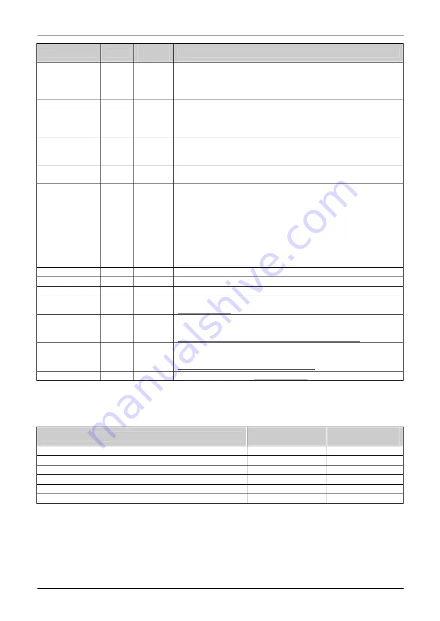
Name
I/O
Interfaced
with
Function
COM1~COM16
(COM1~COM24)
O
LCD
Common driver outputs.
Signals that are not used will output the non-selection waveform. For
example, COM9 to COM16 output the non-selection waveform in 1-line
display mode.
COMI1, COMI2
O
LCD
Common driver outputs for ICON.
SEG1~SEG100
(SEG1~SEG80)
O
LCD
Segment driver outputs.
The output map is different from display modes (3-line, 2-line and 1-line)
please refer to Table 9 for detailed output map.
CAP1P, CAP2P,
CAP3P, CAP4P,
CAP1N, CAP2N
Power
Power
For voltage booster circuit (VDD-VSS).
External capacitor about 0.1uF~4.7uF.
VOUT
Power
Power
Built-in Voltage Booster output.
If using external booster circuit, this pin is used as the power input.
V0~V4
Power
Power
Power supply for LCD drive
V0: built-in Voltage Regulator output.
If using external regulator circuit, this pin is used as the power input.
Internal regulator programmable range: V0 - VSS = 7V (Max);
External power endurance: V0 - VSS = 12V (Max).
V1~V4: built-in voltage follower outputs.
If using external follower circuit, connect the external power to these pins.
Please always keep the voltage relation between these pins to be:
VOUT > V0 > V1 > V2 > V3 > V4 > VSS
VDD
Power
Power
Power for digital circuits. Connect to 1.8V~3.3V power source.
VDD2
Power
Power
Power for analog circuit. Connect to 1.8V~3.3V power source.
VSS
Power
Power
Ground.
VRS
Power
Power
Reserved to monitor the internal Voltage Regulator reference level.
Must be left open.
CLS
I
Option
Select to use internal/external oscillation system.
0: External clock will be input through OSC pin;
1: Using internal clock and the OSC pin must be fixed to VDD.
OSC
I
Oscillation
External clock input pin.
If using external clock, connect this pin to the clock source.
If using internal clock, connect this pin to VDD.
TEST0~TEST5
-
Test Only
Reserved for testing only. Must be left open.
Notes:
1.
Please connect all unused input pins to VDD.
2.
The microprocessor interface pins (CSB, /WR, /RD, A0 and D7~D0) should not be left floating in any operation mode.
Recommended ITO Resistance Limitation
PIN Name
ITO Resistance
(VDD2
≥
2.4V)
ITO Resistance
(VDD2 < 2.4V)
PS2~PS0, CLS, OSC
*1
No Limitation
No Limitation
TEST0~TEST5, VRS
Floating
Floating
VDD, VDD2, VSS, VOUT
<100
Ω
<80
Ω
A0, /WR(R/W), /RD(E), CSB, DB0~DB7
*2
,
<1K
Ω
<800
Ω
V0~V4, CAP1P, CAP1N, CAP2P, CAP2N, CAP3P, CAP4P
<500
Ω
*3
<200
Ω
*3
XRESET
<10K
Ω
*4
<8K
Ω
*4
Notes:
1.
If using internal clock, OSC is connect to VDD and there will be
“
No Limitation
”
on its ITO resistance.
If using external clock, the ITO resistance of OSC should be kept lower than 500
Ω
to control the clock signal quality.
2.
If using I
2
C interface mode, the resistance of SDA signal should be lower than 300
Ω
.
3.
To get a better power system efficiency, the recommended ITO resistance value should be lower than 300
Ω
.