Obsolete Product(s) - Obsolete Product(s)
L6917B
18/33
– Z
F
(s) is the compensation network impedance;
– Z
L
(s) is the parallel of the two inductor impedance;
– A(s) is the error amplifier gain;
–
· is the ACM PWM transfer function where DVosc is the oscillator ramp amplitude
and has a typical value of 2V
Removing the dependence from the Error Amplifier gain, so assuming this gain high enough, the control loop
gain results:
With further simplifications, it results:
Considering now that in the application of interest it can be assumed that Ro>>R
L
; ESR<<Ro and
R
DROOP
<<Ro, it results:
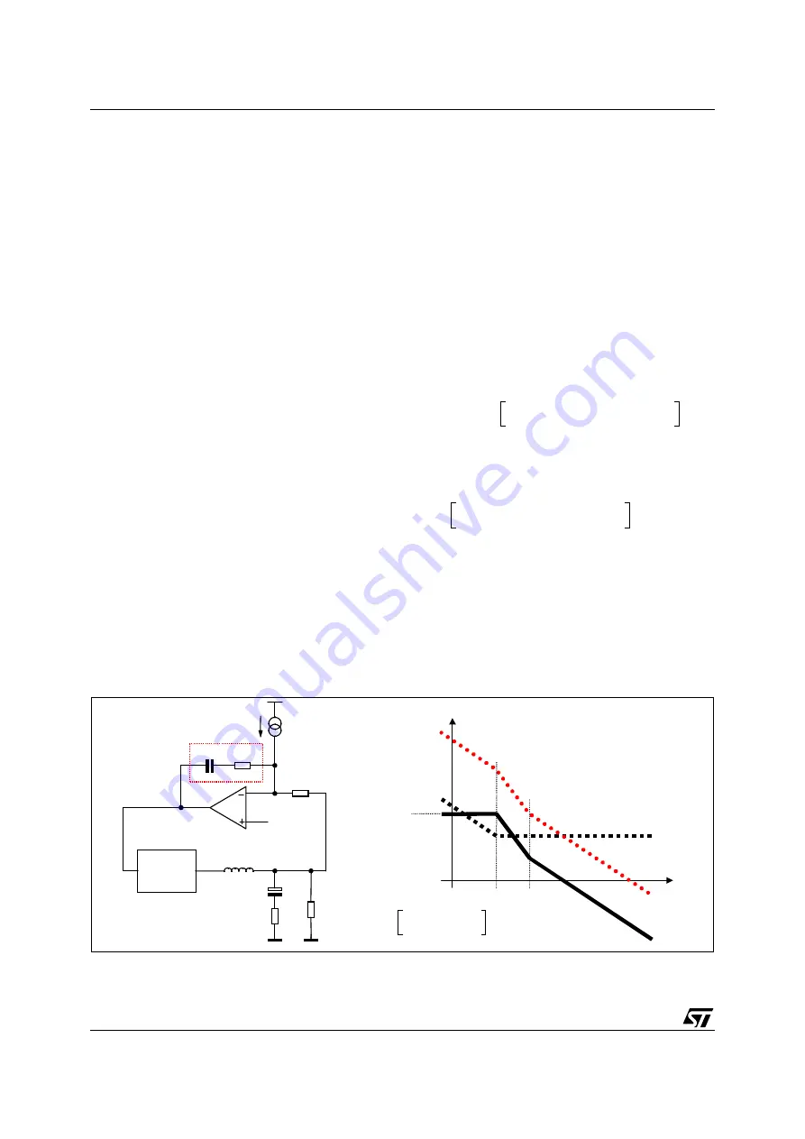
The ACM control loop gain is designed to obtain a high DC gain to minimize static error and cross the 0dB axes
with a constant -20dB/dec slope with the desired crossover frequency
ω
T
. Neglecting the effect of Z
F
(s), the
transfer function has one zero and two poles. Both the poles are fixed once the output filter is designed and the
zero is fixed by ESR and the Droop resistance. To obtain the desired shape an R
F
-C
F
series network is consid-
ered for the Z
F
(s) implementation. A zero at
ω
F
=1/R
F
C
F
is then introduced together with an integrator. This in-
tegrator minimizes the static error while placing the zero in correspondence with the L-C resonance a simple -
20dB/dec shape of the gain is assured (See Figure 12). In fact, considering the usual value for the output filter,
the LC resonance results to be at frequency lower than the above reported zero.
Figure 12. ACM Control Loop Gain Block Diagram (left) and Bode Diagram (right)
Compensation network can be simply designed placing
ω
Z
=
ω
LC
and imposing the cross-over frequency
ω
T
as
desired obtaining:
PWM
4
5
---
V
IN
∆
V
O SC
∆
-------------------
⋅
=
G
LO O P
s
( )
4
5
---
V
IN
V
OS C
∆
-------------------
Z
F
s
( )
Z
P
s
( )
Z
L
s
( )
+
------------------------------------
Rs
Rg
--------
Z
P
s
( )
R
FB
---------------
+
⋅
⋅
⋅
–
=
G
L OO P
s
( )
4
5
---
V
IN
V
O SC
∆
-------------------
Z
F
s
( )
R
FB
---------------
R o
R
D R O OP
+
R o
R
L
2
-------
+
--------------------------------------
1
s Co
R
D R O O P
//Ro
ESR
+
(
)
⋅
⋅
+
s
2
C o
L
2
---
s
L
2 R o
⋅
---------------
Co ESR
Co
R
L
2
-------
⋅
+
⋅
+
1
+
⋅
+
⋅
⋅
----------------------------------------------------------------------------------------------------------------------------------
⋅
⋅
⋅
⋅
–
=
G
L OO P
s
( )
4
5
---
V
IN
V
O SC
∆
-------------------
Z
F
s
( )
R
FB
---------------
1
s Co
R
D R O O P
ESR
+
(
)
⋅
⋅
+
s
2
Co
L
2
---
s
L
2 Ro
⋅
---------------
C o ESR
C o
R
L
2
-------
⋅
+
⋅
+
1
+
⋅
+
⋅
⋅
----------------------------------------------------------------------------------------------------------------------------------
⋅
⋅
⋅
–
=
Rout
Cout
ESR
L/2
R
FB
R
F
C
F
REF
PWM
I
FB
V
COMP
V
OUT
d
•
V
IN
Z
F
dB
ω
ω
T
ω
Z
ω
LC
G
LOOP
Z
F
(s)
K
K
4
5
---
V
IN
V
o sc
∆
---------------
1
R
FB
----------
⋅
⋅
dB
=
Obsolete Product(s) - Obsolete Product(s)


