


PulseBlasterDDS-I-300
Each pin on an IDC header corresponds to a bit in the flag field of an instruction. The association between bits and
pins is shown in the table below (Table 5, next page). In the PBDDS-I-300 design, the flag bits that are used to select
frequency and phase registers are also routed to the IDC connectors so external hardware can be used to determine the
state of the program.
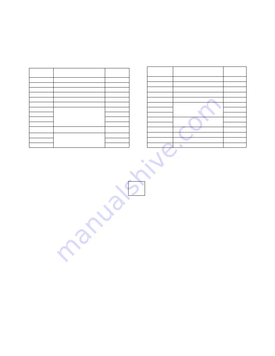
Table 5:
IDC connector pin out.
HWTrig/Reset Header
Figure 13 presents the layout of the short 2x2 IDC header that is the Hardware Trigger/Reset connector. This is an
input connector, for hardware triggering (HW_Trigger) and resetting (HW_Reset). Pins 3 and 4 are grounds, and pins 1
and 2 are the reset and trigger inputs, respectively. Both inputs are pulled high by an on board 10kΩ pull up resistor.
HW_Trigger
(pin 2) When this input detects a falling edge (for example by shorting it with pin 4), a hardware trigger is
produced. This has the same effects as issuing a trigger through software, although the hardware trigger is more precise,
since there are no software latencies involved.
HW_Reset
(pin 1) When this input detects a falling edge (for example by shorting it with pin 3), the pulse program is
reset.
http://www.spincore.com
21
2017-11-14
Figure 13:
HWTrig/Reset
Header pinout.
4
2
3
1
Function
N/A
Ground
14-26
N/A
Unused
13
23
Digital output 8
12
22
Digital output 7
11
21
Digital output 6
10
20
Digital output 5
9
19
TX phase register select
8
18
7
17
6
16
5
15
tx_enable
4
14
Frequency register select
3
13
2
12
1
Bit in
flag word
Pin on
Flag12..23
Function
N/A
Ground
14-26
N/A
Unused
13
11
Frequency register select
12
10
Digital output 4
11
9
phase_reset
10
8
Shape period select
9
7
8
6
7
5
Amplitude select
6
4
5
3
Digital output 3
4
2
Digital output 2
3
1
Digital output 1 (BNC1)
2
0
Digital output 0 (BNC0)
1
Bit in flag
word
Pin on
Flag0..11


