Installation and Instruction Manual - Series 230
Page 7
118128-001 Rev A
The high voltage output connector is located on
the rear panel. An appropriate shielded mating
connector is supplied with each unit. These
connectors are as listed in Table 2.3. Refer to
pages 13-16 for the mating connector assembly
instructions. Only the proper mating connector
should be used with the indicated power supply
and the power supply should never be energized
without a mating connector and suitable load
connected.
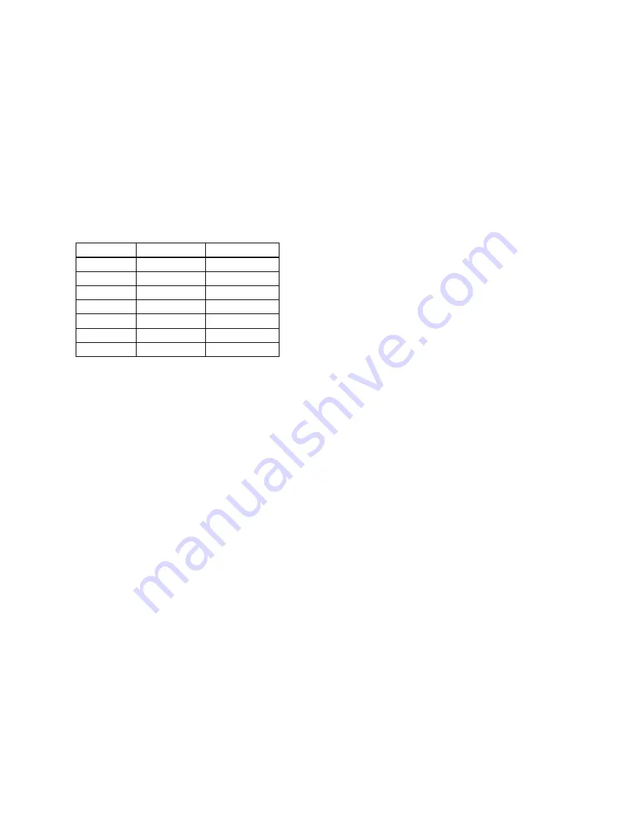
TABLE 2.3: SERIES 230 HIGH VOLTAGE
CONNECTORS
MODEL OUTPUT MATING
-01R JDK PDB
-03R JDK
PDB
-05R JDK
PDB
-10R JJA
405787
-20R JJA
405787
-30R JJA
405787
-50R JJB
405786
SECTION 3
THEORY OF OPERATION
3.1 FUNCTIONAL DESCRIPTION
The circuit uses a DC to DC converter that
converts low voltage DC power to a high
voltage DC output. This output voltage is
highly regulated and filtered and can be varied
either by the front panel controls or through the
REMOTE PROGRAM input on the rear panel.
The input to the DC to DC converter is obtained
from internal low voltage power supplies
powered by the AC line input.
An oscillator determines the frequency
(approximately 20kHz) at which all
amplification, high voltage transformation,
rectification and filtering occurs. The
amplification is a function of a control voltage
that performs the function of control and
regulation. A sample of the output voltage is
compared against a reference voltage in the
sensing circuit. The sensing circuit generates
the control voltage to set and maintain a fixed
high voltage output.
3.2 CIRCUIT DESCRIPTION
The input AC line is converted to the B+
(36Vdc) supply and reg12Vdc low
voltage power supplies. The B+ supply is a
filtered full wave rectifier circuit located on the
chassis. The regulated low voltage power
supply circuit (+12Vdc) consists of a rectifier
circuit located on T1 and output regulators
located on the PCB 100.
The output of the oscillator circuit is amplified
in the AGC amplifier. The gain of the AGC
amplifier is a function of the control voltage
developed at the output of the error amplifier.
The encapsulated high voltage assembly
includes a high voltage power transformer,
rectifier or multiplier circuits, ripple filter and
sensing circuits. These are all critical custom
designed and encapsulated components.
A sample of the high voltage DC output is fed to
the output voltage sensing circuit and is
compared to a command voltage. Output
voltage control is obtained by varying the
command voltage fed to the error amplifier. The
error amplifier compares the command voltage
and the signal from the output voltage sense
circuit. Any difference causes a correction in
the gain control of the AGC amplifier. The
command voltage is controlled by the front
panel controls when the rear panel program
switch is in the LOCAL position.
The reference and reference control and buffer
provide a 5Vdc to the front panel output
voltage controls.
The current sensing circuit monitors the output
current. The buffered output of this circuit is
employed for both internal and remote current
monitoring.
3.3 CURRENT CAPABILITY
The maximum current rating for each model, as
shown in the table to the left, is applicable when
the unit is operated at maximum output voltage.
When operated at reduced output voltage levels,
or when operating in a current limit mode for
charging capacitors, the output current must be
limited to reduced levels. This is required to
protect against excessive power dissipation of
the driver transistors.
The maximum output current must be linearly
derated from maximum output voltage to 30% of