


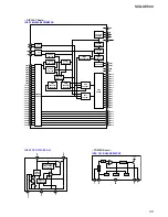
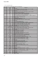


SCD-XE800
31
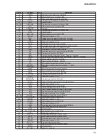
Pin No.
Pin Name
I/O
Description
65 to 73
No Use
O
Not used
74
KEY_INT
I
Wake up signal input terminal
75
LED_LAT
O
Serial data latch pulse signal output terminal Not used
76
No Use
O
Not used
77
No Use
I
I2C Two-way data bus with the clock generator Fixed at “H” in this set
78
No Use
I
I2C data transfer clock signal input/output with the clock generator Fixed at “H” in this set
79 to 82
No Use
O
Not used
83
CKSW
I
Chucking detection switch input terminal
84
OCSW
I
Disc tray open/close detection switch input terminal “L”: disc tray is closed
85
No Use
O
Not used
86
No Use
O
Not used
87
No Use
O
Not used
88
DAC_CS1
O
Chip select signal output to the D/A converter
89
LED_PLAY
O
Play LED drive signal output terminal “H”: LED on
90
LED_PAUSE
O
Pause LED drive signal output terminal “H”: LED on
91
No Use
O
Fixed at “L” in this set
92
DESTINATION
I
Setting terminal for the destination
93
MODEL
I
Setting terminal for the model
94, 95
KEY2, KEY1
I
Front panel key input terminal
96
AVss
-
Ground terminal
97
KEY0
I
Front panel key input terminal
98
Vref
I
Reference voltage (+3.3V) input terminal
99
AVcc
-
Power supply terminal (+3.3V)
100
No Use
O
Not used
Summary of Contents for SCD-XE800
Page 4: ... Bottom view ...
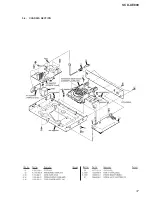
Page 6: ...SCD XE800 2 3 POWER BOARD 2 4 PANEL LOADING 6 ...
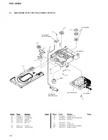
Page 7: ...SCD XE800 2 5 FRONT PANEL BLOCK 2 6 CD MECHANISM DECK BLOCK CDM66F1 DVBU101 Note 1 ß 7 ...
Page 8: ......
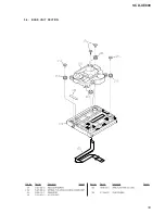
Page 9: ...SCD XE800 2 9 BASE UNIT 2 10 OPTICAL PICK UP BLOCK KHM 313CAB 9 ...
Page 14: ......
Page 15: ......
Page 17: ......
Page 18: ......
Page 19: ......
Page 20: ......
Page 21: ......
Page 22: ......
Page 23: ......
Page 24: ......
Page 25: ......
Page 26: ......
Page 27: ......
Page 37: ...SCD XE800 5 2 CHASSIS SECTION 37 ...
Page 38: ...SCD XE800 5 3 MECHANISM DECK SECTION CDM66F1 DVBU101 38 ...