background image

40

SCD-XE800

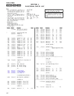
SECTION  6

ELECTRICAL  PARTS  LIST


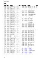
A-1775-568-A  DISPLAY BOARD, COMPLETE


***********************

*


4-945-292-01  HOLDER, 

INDICATION 

TUBE


4-949-935-41 CUSHION 

(FL)


< CAPACITOR >

 C803  1-162-970-11  CERAMIC 

CHIP 0.01uF  10%  25V

 C804  1-126-157-11  ELECT 

10uF 

20%  16V

 C806  1-162-962-11  CERAMIC 

CHIP 470PF 

10%  50V

 C807  1-162-962-11  CERAMIC 

CHIP 470PF 

10%  50V

 C808  1-162-962-11  CERAMIC 

CHIP 470PF 

10%  50V

 C809  1-162-970-11  CERAMIC 

CHIP 0.01uF  10%  25V

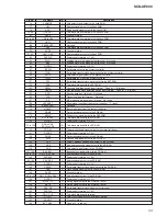
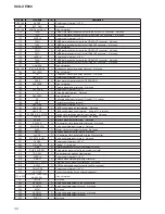
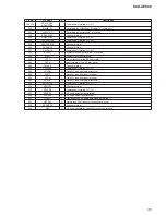
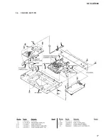
 C810  1-162-923-11  CERAMIC 

CHIP 47PF 

5% 

50V

 C811 

1-126-157-11  ELECT 

10uF 

20%  16V

 C812  1-100-597-91 CERAMIC 

CHIP 0.1uF 

10%  25V

 C813  1-100-597-91 CERAMIC 

CHIP 0.1uF 

10%  25V

 C814  1-100-597-91 CERAMIC 

CHIP 0.1uF 

10%  25V

 C815  1-100-597-91 CERAMIC 

CHIP 0.1uF 

10%  25V

 C816  1-162-970-11  CERAMIC 

CHIP 0.01uF  10%  25V

 C817  1-162-970-11  CERAMIC 

CHIP 0.01uF  10%  25V

 C818  1-115-339-11  CERAMIC 

CHIP 0.1uF 

10%  50V


< CONNECTOR >


CN803 

1-779-552-21 

CONNECTOR, FFC (LIF (NON-ZIF)) 15P


< DIODE >


D801 

6-502-961-01 

DIODE   DA2J10100L


D802 

8-719-046-41 

LED   SEL5521C-TP15 (

B

)


D803 

8-719-046-39 

LED   SEL5821A-TP15 (

X

)


< IC >


IC801 

6-600-767-01 

IC   PNA4823M02S0


IC802 

6-705-899-01 

IC   ML9208-03MBZ03B


IC803 

6-702-302-01 

IC   TK11133CSCL-G


< FLUORESCENT INDICATOR TUBE >

 ND801  1-483-035-11  INDICATOR 

TUBE, 

FLUORESCENT


TRANSISTOR 

>

 Q802  8-729-038-23 TRANSISTOR  RT1N141C-TP-1
 Q803  8-729-038-23 TRANSISTOR  RT1N141C-TP-1
 Q804  8-729-038-23 TRANSISTOR  RT1N141C-TP-1


< RESISTOR >

 R804  1-216-805-11  METAL 

CHIP  47 

5% 

1/10W

 R807  1-216-809-11  METAL 

CHIP  100 

5% 

1/10W

 R808  1-216-809-11  METAL 

CHIP  100 

5% 

1/10W

 R809  1-216-809-11  METAL 

CHIP  100 

5% 

1/10W

 R810  1-216-821-11  METAL 

CHIP  1K 

5% 

1/10W

 R811 

1-216-827-11  METAL 

CHIP  3.3K 

5% 

1/10W

 R812  1-216-845-11  METAL 

CHIP  100K 

5% 

1/10W

 R813  1-216-821-11  METAL 

CHIP  1K 

5% 

1/10W

 R814  1-216-821-11  METAL 

CHIP  1K 

5% 

1/10W

 R815  1-216-825-11  METAL 

CHIP  2.2K 

5% 

1/10W

 R816  1-216-815-11  METAL 

CHIP  330 

5% 

1/10W

 R817  1-216-817-11  METAL 

CHIP  470 

5% 

1/10W


< ROTARY ENCODER >

 S806  1-477-995-11  ENCODER, 

ROTARY 

(

AMS 

>

 PUSH ENTER)


< SWITCH >

 S807  1-771-410-21 SWITCH, 

TACTILE 

(

Z

)

 S808  1-771-410-21 SWITCH, 

TACTILE 

(

B

)

 S809  1-771-410-21 SWITCH, 

TACTILE 

(

X

)

 S810  1-771-410-21 SWITCH, 

TACTILE 

(

x

)

************************************************************


KEY 

BOARD


*********


< CONNECTOR >


CN809 

1-564-718-11 

PIN, CONNECTOR (SMALL TYPE) 2P


< RESISTOR >

 R801  1-216-821-11  METAL 

CHIP  1K 

5% 

1/10W

 R802  1-216-825-11  METAL 

CHIP  2.2K 

5% 

1/10W

 R803  1-216-825-11  METAL 

CHIP  2.2K 

5% 

1/10W


< SWITCH >

 S801  1-771-410-21 SWITCH, 

TACTILE 

(l/

1

)

 S802  1-771-410-21 SWITCH, 

TACTILE 

(SA-CD/CD)

 S803  1-771-410-21 SWITCH, 

TACTILE 

(TIME/TEXT


S804 

1-771-410-21 

SWITCH, TACTILE (DISPLAY MODE)

************************************************************


A-1775-565-A  MAIN BOARD, COMPLETE


********************


< CAPACITOR >

 C201  1-115-156-11  CERAMIC 

CHIP 1uF 


10V

  Ref. No. 

Part No. 

Description 

Remark

  Ref. No. 

Part No. 

Description 

Remark

KEY

MAIN

DISPLAY

When indicating parts by reference num-
ber, please include the board name.

Note:
•  Due to standardization, replacements in 

the parts list may be different from the 
parts specifi ed in the diagrams or the com-
ponents used on the set.

•  -XX and -X mean standardized parts, so 

they may have some difference from the 
original one.

•  Items marked “

*

” are not stocked since 

they are seldom required for routine ser-
vice. Some delay should be anticipated 
when ordering these items.

• RESISTORS
  All resistors are in ohms.
 METAL: 

Metal-fi lm resistor.

  METAL OXIDE: Metal oxide-fi lm resistor.
 F: 

nonfl ammable

• CAPACITORS
 uF: 

µ

F

• COILS
 uH: 

µ

H

• SEMICONDUCTORS
  In each case, u: 

µ

, for example:

 uA. 

. : 

µ

A. . , uPA. . , 

µ

PA. . , 

 uPB. 

µ

PB. . , uPC. . , 

µ

PC. . , 

 uPD. 

µ

PD. .

The components identifi ed by mark 

0


or dotted line with mark 

0

 are critical for 

safety.
Replace only with part number specifi ed.

Summary of Contents for SCD-XE800

Page 1: ...eral Laser Diode Properties Emission duration Continuous Laser Output Less than 44 6 µW This output is the value measurement at a distance of 200 mm from the objective lens surface on the Optical Pick up Block with 7 mm aperture Power requirements 230 V AC 50 60 Hz Power consumption 20 W Power consumption during standby mode 0 5 W Dimensions w h d 430 95 295 mm incl projecting parts Mass approx 3 ...

Page 2: ...Chassis Section 37 5 3 Mechanism Deck Section CDM66F1 DVBU101 38 5 4 Base Unit Section 39 6 ELECTRICAL PARTS LIST 40 Accessories are given in the last of the electrical parts list TABLE OF CONTENTS NOTES ON CHIP COMPONENT REPLACEMENT Never reuse a disconnected chip component Notice that the minus side of a tantalum capacitor may be dam aged by heat FLEXIBLE CIRCUIT BOARD REPAIRING Keep the tempera...

Page 3: ...added to ordinary solder ABOUT THE REMOTE COMMANDER USED IN THE SERVICE MODE When the service mode is operated the following remote com mander is necessary The service mode cannot be operated by remote commander to which this machine is attached Remote commander RM ASP004 Part No 1 479 272 21 Note Above mentioned remote commander is one example If it is the one printed under a remote commander as ...

Page 4: ... Bottom view ...

Page 5: ...01 SET 2 3 POWER BOARD Page 6 2 10 OPTICAL PICK UP BLOCK KHM 313CAB Page 9 2 7 MAIN BOARD Page 8 2 9 BASE UNIT Page 9 2 5 FRONT PANEL BLOCK Page 7 2 6 CD MECHANISM DECK BLOCK CDM66F1 DVBU101 Page 7 2 8 BELT LD MOTOR BOARD MOTOR L ASSY LOADING M001 Page 8 2 4 PANEL LOADING Page 6 2 2 CASE FUSE F001 Page 5 5 case 6 fuse F001 3 3 4 1 two screws case 3 TP2 1 two screws case 3 TP2 2 screw BVTP3 8 ...

Page 6: ...SCD XE800 2 3 POWER BOARD 2 4 PANEL LOADING 6 ...

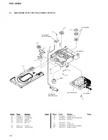
Page 7: ...SCD XE800 2 5 FRONT PANEL BLOCK 2 6 CD MECHANISM DECK BLOCK CDM66F1 DVBU101 Note 1 ß 7 ...

Page 8: ......

Page 9: ...SCD XE800 2 9 BASE UNIT 2 10 OPTICAL PICK UP BLOCK KHM 313CAB 9 ...

Page 10: ...en all keys are pressed correctly K9 and OK are alternately displayed 8 When the AMS PUSH ENTER dial on the set is turned in the direction of right J0 is changed to J1 then J9 When the AMS PUSH ENTER dial on the set is turned in the direction of left J0 is changed to J9 then J0 9 To release from this mode press three buttons in the same manner as step 2 Note 1 According to the following procedures...

Page 11: ...de of MTK changed without permission 2Gnnn Reacts to the key notification no though the communication with MTK is alive Serial communications MTK communication error factor Test key3 t 3Annn It was not possible to communicate with MTK with 48ms 3Bnnn A non standard packet length was received Excluding 16 bytes 3Cnnn Checksum NG 3Dnnn Type of the communication header is NG MTK power control Power O...

Page 12: ... xxxxx IF con Ver xx xx xxxx Syscon Ver x xxx 4 To execute each function press its number by using numeric button on the remote commander 5 To release from this mode disconnect the power cord Note Don t press the 1 button when to release from this mode Nec essarily disconnect the power cord The set doesn t operate when turning off power with 1 button of the set 3 Executing IOP Measurement In order...

Page 13: ...ment error 31 DPD offset adjustment error 32 TE balance adjustment error 33 TE sensor adjustment error 34 TE loop gain adjustment error 35 FE loop gain adjustment error 36 Bad jitter after adjustment 40 Focus NG 42 Focus layer jump NG 51 Spindle stop error 52 Open kick spindle error 60 Focus on error 61 Seek fail error 62 Read Q data ID error 70 Lead in data read fail 71 TOC read time out CD 80 Ca...

Page 14: ......

Page 15: ......

Page 16: ...production tolerances Circled numbers refer to waveforms Signal path F SA CD PLAY J CD PLAY ANALOG c CD PLAY DIGITAL For Printed Wiring Boards Note X Parts extracted from the component side Y parts extracted from the conductor side f internal component Pattern from the side which enables seeing The other layers patterns are not indicated Caution Pattern face side Conductor Side Parts face side Com...

Page 17: ......

Page 18: ......

Page 19: ......

Page 20: ......

Page 21: ......

Page 22: ......

Page 23: ......

Page 24: ......

Page 25: ......

Page 26: ......

Page 27: ......

Page 28: ... F MUX MODE CONTROL IC203 1202 TK11150CSCL G IC204 1105 1107 TK11133CSCL G CONTROL CIRCUIT BANDGAP REFERENCE OVERHEAT OVERCURRENT PROTECTION 1 VCONT 3 NP 2 GND 4 VOUT 5 VIN IC503 PST8435UL IC504 506 SI 3010KM TLS IC1902 SM8707EV G E2 IC1901 TC74LVX4053FT EL GND 1 VDD 2 VREF OUT 4 CD 3 1 VC TSD 2 VIN 3 GND 4 VOUT 5 ADJ REF 1 VDD1 2 VSS1 3 MO1 4 MO2 5 VDD2 6 VSS2 7 XTI 8 XTO 16 NC 15 SO2 14 FSEL 13 ...

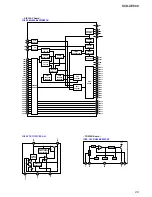
Page 29: ... 11 SEG7 12 SEG8 13 SEG9 14 SEG10 15 SEG11 16 SEG12 17 SEG13 18 SEG14 19 SEG15 20 SEG16 21 SEG17 22 SEG18 23 SEG19 24 SEG20 25 SEG21 26 SEG22 27 SEG23 28 SEG24 29 SEG25 30 SEG26 31 SEG27 32 SEG28 SEGMENT DRIVER ADRAM 16W 2B CGRAM 248W 35B DCRAM 16W 8B ADDRESS SELECTOR READ ADDRESS COUNTER WRITE ADDRESS COUNTER CGRAM 8W 35B CONTROL CIRCUIT TIMING GENERATOR1 OSCILLATOR TIMING GENERATOR2 DIGIT CONTRO...

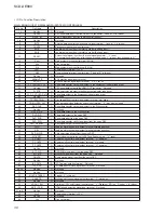
Page 30: ...d 27 CDM_OPEN_SW I Disc tray open close detection switch input terminal L disc tray is closed 28 DAC_CLK O Serial data transfer clock signal output to the D A converter 29 No Use I Not used 30 DAC_DATA O Serial data output to the D A converter 31 DVD_SID O Serial data output to the servo DSP 32 DVD_SOD I Serial data input from the servo DSP 33 DVD_SCO I Serial data transfer clock signal input from...

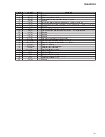
Page 31: ...W I Disc tray open close detection switch input terminal L disc tray is closed 85 No Use O Not used 86 No Use O Not used 87 No Use O Not used 88 DAC_CS1 O Chip select signal output to the D A converter 89 LED_PLAY O Play LED drive signal output terminal H LED on 90 LED_PAUSE O Pause LED drive signal output terminal H LED on 91 No Use O Fixed at L in this set 92 DESTINATION I Setting terminal for t...

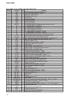
Page 32: ...k up block 29 VREFO O Reference voltage 1 4V output terminal 30 FEO O Focus error monitor output terminal Not used 31 TEO O Tracking error monitor output terminal Not used 32 TEZISLV O O Slice level of tracking error signal output terminal Not used 33 OP_OUT O Output to the internal operational amplifier Not used 34 OP_INN I Negative input from the internal operational amplifier Not used 35 OP_INP...

Page 33: ... signal input from the system controller L reset 109 RESERVED Not used 110 xIFBSY I Busy signal input from the system controller 111 DQM0 O Data mask signal output to the SD RAM 112 EEWP O Write protect signal output to the EEPROM 113 to 117 RD7 to RD3 I O Two way data bus with the SD RAM 118 DVDD3 Power supply terminal 3 3V 119 to 129 RD2 to RD0 RD15 to RD8 I O Two way data bus with the SD RAM 13...

Page 34: ... supply terminal 3 3V 196 VBUS_OE O VBUS control signal output terminal Not used 197 VBUS_OC I VBUS control signal input terminal Fixed at H in this set 198 SCORE DIR_XSTATE I Source clock switching monitor input terminal Not used 199 SPMCK O Master clock signal output terminal Not used 200 SPBCK O Bit clock signal output terminal Not used 201 SPLRCK O L R sampling clock signal output terminal Not...

Page 35: ... of the RF jitter meter 241 JITFN I Input terminal of the RF jitter meter 242 PLLVSS Ground terminal 243 PLLVDD3 Power supply terminal 3 3V 244 LPFON O Data PLL loop filter output terminal 245 LPFIP I Data PLL loop filter input terminal 246 LPFIN I Data PLL loop filter input terminal 247 LPFOP O Data PLL loop filter output terminal 248 ADCVDD3 Power supply terminal 3 3V 249 ADCVSS Ground terminal ...

Page 36: ... for routine ser vice Some delay should be anticipated when ordering these items The mechanical parts with no reference number in the exploded views are not sup plied Color Indication of Appearance Parts Ex ample KNOB BALANCE WHITE RED 5 1 CASE FRONT PANEL SECTION The components identiÞed by mark or dotted line with mark are critical for safety Replace only with part number speciÞed 36 ...

Page 37: ...SCD XE800 5 2 CHASSIS SECTION 37 ...

Page 38: ...SCD XE800 5 3 MECHANISM DECK SECTION CDM66F1 DVBU101 38 ...

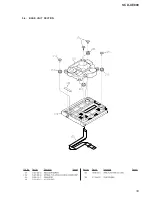
Page 39: ...SCD XE800 5 4 BASE UNIT SECTION 39 ...

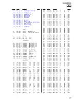
Page 40: ...HIP 100K 5 1 10W R813 1 216 821 11 METAL CHIP 1K 5 1 10W R814 1 216 821 11 METAL CHIP 1K 5 1 10W R815 1 216 825 11 METAL CHIP 2 2K 5 1 10W R816 1 216 815 11 METAL CHIP 330 5 1 10W R817 1 216 817 11 METAL CHIP 470 5 1 10W ROTARY ENCODER S806 1 477 995 11 ENCODER ROTARY AMS PUSH ENTER SWITCH S807 1 771 410 21 SWITCH TACTILE Z S808 1 771 410 21 SWITCH TACTILE B S809 1 771 410 21 SWITCH TACTILE X S810...

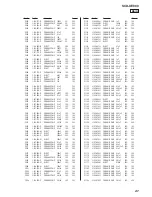
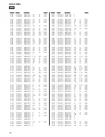
Page 41: ... CHIP 0 01uF 10 25V C1108 1 162 970 11 CERAMIC CHIP 0 01uF 10 25V C1110 1 165 908 11 CERAMIC CHIP 1uF 10 10V C1111 1 104 658 91 ELECT 100uF 20 10V C1112 1 126 947 11 ELECT 47uF 20 35V C1113 1 162 970 11 CERAMIC CHIP 0 01uF 10 25V C1114 1 107 826 11 CERAMIC CHIP 0 1uF 10 16V C1115 1 107 826 11 CERAMIC CHIP 0 1uF 10 16V C1116 1 107 826 11 CERAMIC CHIP 0 1uF 10 16V C1117 1 126 947 11 ELECT 47uF 20 35...

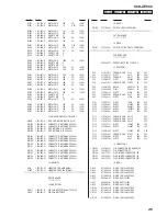
Page 42: ...IC CHIP 0 01uF 10 25V C2108 1 127 760 11 CERAMIC CHIP 4 7uF 10 6 3V C2109 1 104 658 91 ELECT 100uF 20 10V C2110 1 104 658 91 ELECT 100uF 20 10V C2114 1 107 826 11 CERAMIC CHIP 0 1uF 10 16V C2115 1 165 989 11 CERAMIC CHIP 10uF 10 6 3V C2116 1 107 826 11 CERAMIC CHIP 0 1uF 10 16V C2117 1 165 989 11 CERAMIC CHIP 10uF 10 6 3V C2118 1 107 826 11 CERAMIC CHIP 0 1uF 10 16V C2119 1 162 964 11 CERAMIC CHIP...

Page 43: ...K 5 1 10W R286 1 216 809 11 METAL CHIP 100 5 1 10W R287 1 216 809 11 METAL CHIP 100 5 1 10W R288 1 216 809 11 METAL CHIP 100 5 1 10W R289 1 216 801 11 METAL CHIP 22 5 1 10W R290 1 216 801 11 METAL CHIP 22 5 1 10W R291 1 216 801 11 METAL CHIP 22 5 1 10W R292 1 216 801 11 METAL CHIP 22 5 1 10W R293 1 216 801 11 METAL CHIP 22 5 1 10W R294 1 216 801 11 METAL CHIP 22 5 1 10W R295 1 216 801 11 METAL CHI...

Page 44: ...1 1 216 833 11 METAL CHIP 10K 5 1 10W R1152 1 216 864 11 SHORT CHIP 0 R1153 1 216 864 11 SHORT CHIP 0 R1154 1 216 864 11 SHORT CHIP 0 R1155 1 216 864 11 SHORT CHIP 0 R1156 1 216 809 11 METAL CHIP 100 5 1 10W R1159 1 216 833 11 METAL CHIP 10K 5 1 10W R1160 1 216 805 11 METAL CHIP 47 5 1 10W R1161 1 216 805 11 METAL CHIP 47 5 1 10W R1162 1 216 833 11 METAL CHIP 10K 5 1 10W R1163 1 216 833 11 METAL C...

Page 45: ...B1114 1 234 400 21 CONDUCTOR NETWORK 1005X4 RB1115 1 234 400 21 CONDUCTOR NETWORK 1005X4 VIBRATOR X501 1 795 121 21 VIBRATOR CERAMIC 5MHz X1900 1 813 218 21 VIBRATOR CRYSTAL 27MHz MOTOR BOARD CONNECTOR CN010 1 564 721 11 PIN CONNECTOR SMALL TYPE 5P CN011 1 506 481 11 PIN CONNECTOR 2P SWITCH SW010 1 572 086 11 SWITCH LEAF CHUCKING OUT SW BOARD SWITCH SW011 1 762 424 11 SWITCH MICRO TRAY OPEN CLOSE ...

Page 46: ...1 METAL CHIP 150K 5 1 10W R57 1 216 843 11 METAL CHIP 68K 5 1 10W 0 R60 1 249 389 91 CARBON 4 7 5 1 4W F R61 1 216 819 11 METAL CHIP 680 5 1 10W R101 1 216 833 11 METAL CHIP 10K 5 1 10W R102 1 216 833 11 METAL CHIP 10K 5 1 10W 0 R103 1 249 423 91 CARBON 3 3K 5 1 4W F R104 1 216 809 11 METAL CHIP 100 5 1 10W R105 1 216 809 11 METAL CHIP 100 5 1 10W R106 1 216 837 11 METAL CHIP 22K 5 1 10W R107 1 21...

Reviews: