


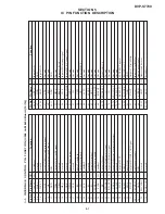


5-2
1
PB14/IRQ6
I
Input of interrupt fromIC506
2
PB15/IRQ7
I
Input of interrupt fromIC804
3
VSS
–
Digital ground
4-11
AD0-7
I/O
Data bus
AD0-7
12
VSS
–
Digital ground
13, 14
AD8, 9
I/O
Data
bus
AD8,9
15
VCC
–
Digital power supply
16-21
AD10-15
I/O
Data bus
AD10-15
22
VSS
–
Digital ground
23-30
A0-7
O
Addres bus
A0-7
31
VSS
–
Digital ground
32-39
A8-15
O
Addres bus
A8-15
40
VSS
–
Digital ground
41, 42
A16, 17
O
Addres
bus
A16,17
43
VCC
–
Digital power supply
44-47
A18-21
O
Addres bus
A18-21
48
CS0
O
Chip select signal for external ROM(ICS803)
49
CS1
O
Chip select signal for external ROM(IC802)
50
CS2
–
Not used
51
CS3
–
Not used
52
VSS
–
Digital ground
53
P
A0/CS4
O
Reset signal for IC101,209
54
P
A1/CS5
O
Output of reset signal
55
P
A2/CS6
O
Output of chip select signal to IC804
56
W
AIT
I
Input of wait signal
57
WRL/WR
O
Output of write signal
58
WRH/LBS
–
Not used
59
RD
O
Output of read signal
6
0
P
A7/BACK
O
Output of reset signal to IC508
61
VSS
–
Digital ground
62
P
A8/BREQ
O
Output of reset signal to IC101
63
P
A
9
O
Output of reset signal to IC506
64
P
A10
O
Output of
A
mute signal
65
P
A
1
1
O
Output of MA mute signal
66
IRQ0
I
Input of interrupt fromIC203
67
IRQ1
I
Input of DMA request from IC203
68
IRQ2
I
Input of
V
SYNC(FID) interrupt signal
69
IRQ3
I
Input of interrupt from IC804
70
VCC
–
Digital power supply
71
CK
O
Output of internal clock
72
VSS
–
Digital ground
73
EXT
AL
–
20MHz crystal connection pin
74
XT
AL
–
20MHz crystal connection pin
75
VCC
–
Digital power supply
76
NMI
I/O
Hyper terminal pin
77
VCC
(Vpp)
–
Digital power supply
78
W
D
T
O
V
F
–
Not used
79
RES
I
Input of reset signal
80
MD0
I
Input of mode select0 (fixed to 1)
81
MD1
I
Input of mode select1 (fixed to 0)
82
MD2
I
Input of mode select2 (fixed to 0)
83,
84
VCC
–
Digital power supply
85
A
VCC
–
Analog power supply
86
A
VREF
–
Reference power supply
87
PC0/AN0
I/O
Set of mode 1
88
PC1/AN1
I/O
Set of mode 2
89
PC2/AN2
I/O
Set of mode 3
90
PC3/AN3
I/O
Set of mode 4
91
A
VSS
–
Analog ground
92
PC4/AN4
I/O
Set of mode 5
93
PC5/AN5
I/O
Set of mode 6
94
PC6/AN6
–
Not used
95
PC7/AN7
–
Not used
96
VSS
–
Digital ground
97
PB0
–
HFG
98
PB1
O
Output of reset signal for IC806
99
VCC
–
Digital power supply
100
PB2
–
Not used
5-2.
SYSTEM CONTR
OL PIN FUNCTION (IC805 on MB-84 Boar
d (13/14))
Pin No.
Pin Name
I/O
Function
Pin No.
Pin Name
I/O
Function
Summary of Contents for DVP-S7700
Page 12: ...1 2 ...
Page 13: ...1 3 ...
Page 14: ...1 4 ...
Page 15: ...1 5 ...
Page 16: ...1 6 ...
Page 17: ...1 7 ...
Page 18: ...1 8 ...
Page 19: ...1 9 ...
Page 20: ...1 10 ...
Page 21: ...1 11 1 11 E ...
Page 36: ...DVP S7700 4 3 4 4 4 1 FRAME SCHEMATIC DIAGRAM 1 2 FRAME 1 2 ...
Page 37: ...DVP S7700 4 5 4 6 FRAME SCHEMATIC DIAGRAM 2 2 FRAME 2 2 ...