background image

– 37 –

7-9.

IC  PIN  FUNCTION  DESCRIPTION

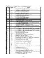
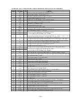
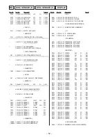
 BD BOARD   IC101   LA9241M (RF AMPLIFIER, FOCUS/TRACKING/SLED SERVO)

Pin No.

Pin Name

I/O

Function

1

FIN2

I

Signal input (B+D) from the optical pick-up detector
Added with FIN1 to create RF signal, subtracted with FIN1 to create focus error signal

2

FIN1

I

Signal input (A+C) from the optical pick-up detector

3

E

I

Signal input (E) from the optical pick-up detector
Subtracted with F to create tracking error signal

4

F

I

Signal input (F) from the optical pick-up detector

5

TB

I

Tracking error signal input for the tracking balance adjustment

6

TE–

I

Tracking error signal (invert signal) input terminal

7

TE

O

Tracking error signal output terminal

8

TESI

I

TES (Track Error Sense) comparator input terminal
Tracking error signal is band-passed and input

9

SCI

I

Shock detection input terminal

10

TH

I

Time constant setting terminal for the tracking gain adjustment

11

TA

O

TA amplifier output terminal

12

TD–

I

Creates a tracking phase compensation constant between TD (pin 

) and VR (pin 

%•

) pins

13

TD

O

Setting terminal for the tracking phase compensation

14

JP

I

Setting terminal for the tracking jump signal (kick pulse) amplitude

15

TO

O

Tracking coil (2-axis device) drive signal output to the LA6541 (IC103), and sled motor drive
signal output terminal

16

FD

O

Focus coil (2-axis device) drive signal output to the LA6541 (IC103)

17

FD–

I

Creates a focusing phase compensation constant between FD (pin 

) and FA (pin 

!•

) pins

18

FA

O

Creates a focusing phase compensation constant between FD– (pin 

) and FA– (pin 

) pins

19

FA–

I

Creates a focusing phase compensation constant between FA (pin 

!•

) and FE (pin 

) pins

20

FE

O

Focus error signal output terminal

21

FE–

I

Focus error signal (invert signal) input terminal

22

AGND

Ground terminal (analog system)

23

SP

O

Single end output of the CV+ (pin 

) and CV– (pin 

) pins signal

24

SPI

I

Spindle amplifier input terminal (invert input)

25

SPG

I

Gain setting resistor is connected when the spindle 12 cm mode

26

SP–

I

Works together with the SPD (pin 

) to connect to the spindle phase compensation constant

27

SPD

O

Spindle motor (M101) drive signal output to the LA6541 (IC103)

28

SLEQ

I

Sled phase compensation constant is connected

29

SLD

O

Sled motor (M102) drive signal output to the LA6541 (IC103)

30

SL–

I

Sled feeding signal input from the system controller (IC801)

31

SL+

I

Sled feeding signal input from the system controller (IC801)

32

JP–

I

Tracking jump control signal input from the DSP (IC102)

33

JP+

I

Tracking jump control signal input from the DSP (IC102)

34

TGL

I

Tracking gain control signal input from the DSP (IC102)    Gain becomes low when TGL is “H”

35

TOFF

I

Tracking off control signal input from the DSP (IC102)
Tracking becomes off when TOFF is “H”

36

TES

O

Tracking error signal output to the DSP (IC102)

37

HFL

O

Tracking detection signal output to the DSP (IC102)    HFL (High Frequency Level) is used to
determine whether the main beam is positioned on a pit or a mirror

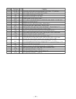
38

SLOF

I

Sled servo off control signal input from the DSP (IC102)    Rough servo/phase control automatic
switching monitor input    “H”: rough servo, “L”: phase servo

39

CV–

I

CLV error signal input from the DSP (IC102)

Summary of Contents for CDP-CX53 - CD Changer

Page 1: ...B S N Jack Maximum Load impedance type output level LINE OUT Phono 2V Over 10 kilohms Jacks at 50 kilohms DIGITAL Optical 18 dBm Wave length 660 nm OUT output OPTICAL connector Where purchased Power requirements USA Canada 120 V AC 60 Hz Australia 240 V AC 50 Hz Europe 220 V 230 V AC 50 60 Hz Other countries 110 V 120 V or 220 V 240 V AC adjustable 50 60 Hz General Power requirements Power consump...

Page 2: ...cated on the rear exterior 4 997 124 01 4 997 124 11 4 997 124 21 4 997 124 31 4 997 124 41 4 997 124 51 US model Canadian model AEP AED model Australian model E model Singapore model PARTS No MODEL MODEL IDENTIFICATION BACK PANEL Abbreviation AED North Europe PARTS No CAUTION INVISIBLE LASER RADIATION WHEN OPEN AND INTERLOCKS DEFEATED AVOID EXPOSURE TO BEAM ADVARSEL USYNLIG LASERSTRÅLING VED ÅBNI...

Page 3: ...rated AC milliammeter The Data Precision 245 digital multimeter is suitable for this job 3 Measuring the voltage drop across a resistor by means of a VOM or battery operated AC voltmeter The limit indica tion is 0 75 V so analog meters must have an accurate low voltage scale The Simpson 250 and Sanwa SH 63Trd are ex amples of a passive VOM that is suitable Nearly all battery operated digital multi...

Page 4: ... REPEAT button 5 Display window 6 BLOCK 1 5 buttons 7 DISC PUSH ENTER knob PUSH OPEN STANDBY I u PULS ONE PLAY MODE REPEAT BLOCK FILE 1 2 3 BLOCK 4 5 CHECK CLEAR PUSH ENTER DISC ª P p 1 2 3 4 5 6 7 8 9 0 LOCATION OF PARTS AND CONTROLS Front Panel 8 CHECK button 9 CLEAR button º button button p button P button button PLUS ONE button ...

Page 5: ...screws M3 8 1 two screws M3 8 4 screw BVTT3 6 3 two screws BVTT3 6 8 three screws BVTT3 6 5 connector CN803 6 wire flat type 15 core CN801 7 wire flat type 9 core CN103 2 case 9 claw 9 claw 0 front panel 1 two screws M3 8 5 table 50 4 screw PTPWH2 6 8 1 screw BVTT3 6 2 connector CN84 3 bracket ILLUMINATION TABLE 50 ...

Page 6: ...w BVTT3 8 1 screw BVTT3 6 9 screw P3 14 6 connector CN53 connector CN61 0 connector CN51 7 wire flat type 12 core CN102 base CDM 4 ring B 8 base LOADING 6 two screws BVTT3 6 1 two screws 4 transformer cover 9 AUDIO board 3 two screws BVTT3 6 1 screw BVTP3 8 8 connector CN701 2 ring A 5 screw BVTT3 6 7 three screws BVTP3 10 ...

Page 7: ...screws PTPWH2 6 8 3 screw BTP2 6 10 2 bracket 4 reinforcement small 5 two tention springs 7 base unit 1 wire flat type 16 core CN101 8 gear cover 2 screw B2 5 7 three claws 4 BD board 3 Removal four solders sled motor M102 0 two screws 2 3 5 claw 9 gear B RP 6 gear A S ...

Page 8: ... 8 OPTICAL PICK UP KSS 213B S N 3 Remove the optical pick up to direction of the arrow A A 1 claw 2 sled shaft ...

Page 9: ...m disc The following special functions will work when certain functions are pressed in this mode Special functions in ADJ mode The buttons function only with the general purpose remote Button Function 3 Tracking servo sled servo OFF 8 Tracking servo sled servo ON CHECK S shape observation mode FLUORESCENT INDICATOR TUBE LED ALL LIT AND KEY CHECK MODE Connect TP AFADJ and ground of the DISPLAY boar...

Page 10: ...eously display the error number and stop opera tions However the stopping conditions differ according to whether the unit is equipped with the self protection function during errors described later The function serves to maintain the state of the unit when errors occur Special Functions in Aging Mode There are some useful function in the aging mode Disc setting mode 1 Switching of use disuse of pr...

Page 11: ...be repeated as long as no errors occur 10 After each aging cycle the number displayed on the Fluores cent indicator tube will increase 11 To end aging press the I u button Error Display Error code Without remote commander for aging mode 1 Turn ON the power of the unit Open the front cover 2 Press the PLAY MODE and buttons in order 3 When the disc set mode is set the and P LEDs blink The following ...

Page 12: ...ame time and turn ON the power 4 The fluorescent indicator tube shows as follows and the mechanism section adjustment mode is set 5 The disc table rotates in the clockwise direction The disc table rotation time is displayed with PLUS ONE slit as a measuring point 6 Measure the waveform of the oscilloscope when the disc table is rotating oscilloscope SENS CH1 TEST CH2 GND SENS GND TEST AUDIO board ...

Page 13: ...top of the SENS CH1 input waveform and the H center of TEST CH2 coincide 10 If the adjustment is not successful press the CLEAR button to rotate the disc table in the clockwise direction and perform steps 6 to 9 Note During the adjustment mode the rotational direction is switched each time the CLEAR button is pressed Pressing the CHECK button enters the loading mode which will be described later P...

Page 14: ...A ALIGMENT 1 Check that there is no disc in the unit and then turn ON the power Open the door and set a disc in the PLUS ONE slit 2 Turn OFF the power close the door and while pressing the CLEAR and PLUS ONE buttons simultaneously turn ON the power again 3 Press the CHECK button and set the loading mode 4 Press the button and chuck the disc 5 Press or button to stop the disc holder A slightly away...

Page 15: ... lead wire 8 Press the I u button and turn ON the power 9 Playback the fifth track of the disc 10 Confirm that oscilloscope waveform is clear and check RF sig nal level is correct or not 11 Turn OFF the power and remove the lead wire connected at step 7 Note A clear RF signal waveform means that the shape can be clearly distinguished at the center of the waveform E F Balance Traverse Check The pro...

Page 16: ...RF PLL Free run Frequency Check Procedure 1 Connect the frequency counter to TP PCK of the BD board 2 Press the I u button and turn ON the power supply 3 Open the front cover and press the PLUS ONE button 4 Set the disc YEDS 18 into the PLUS ONE slit 5 Close the front cover and chuck the disc 6 Playback the fifth track of the disc 7 Confirm that reading on frequency counter is 4 3218 MHz 30 kHz Ab...

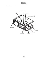
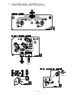
Page 17: ... 17 SECTION 7 DIAGRAMS Circuit Boards Location TABLE SENSOR BOARD DISC SENSOR R board DISC SENSOR S board AUDIO board BD board SW board CD MOTOR board POWER SW board LED board ...

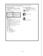
Page 18: ...ur la sécurité Ne les remplacer que par une piéce portant le numéro spécifié U B Line V B Line H adjustment for repair Voltages and waveforms are dc with respect to ground under no signal conditions no mark PLAY Voltages are taken with aVOM Input impedance 10 MΩ Voltage variations may be noted due to normal produc tion tolerances Waveforms are taken with a oscilloscope Voltage variations may be no...

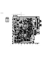
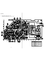
Page 19: ...7 1 PRINTED WIRING BOARD BD Section See page 17 for Circuit Boards Location See page 18 for Note Semiconductor Location Ref No Location D151 D 1 IC101 D 3 IC102 B 3 IC103 B 1 Q101 B 4 Q102 B 4 Q103 E 1 Page 23 Page 28 ...

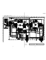
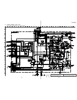
Page 20: ...scription See page 18 for Note no mark PLAY Signal path J CD c digital out 21 22 The components identified by mark or dotted line with mark are critical for safety Replace only with part number specified Les composants identifiés par une marque sont critiques pour la sécurité Ne les remplacer que par une piéce portant le numéro spécifié ...

Page 21: ... IC702 B 3 IC703 B 3 Q301 D 3 Q302 D 5 Q303 D 3 Ref No Location Ref No Location D301 D 3 D701 B 5 D702 B 5 D703 B 5 D704 B 5 D705 C 5 D706 C 5 D707 C 6 D708 C 4 D709 C 5 D811 D 2 Semiconductor Location Q313 D 3 Q401 D 5 Q402 D 5 Q403 D 3 Q413 D 4 Q501 D 5 Q701 D 6 Q821 D 2 Ref No Location 23 24 Page 32 Page 31 Page 28 Page 20 Page 31 Page 31 Page 32 Page 28 ...

Page 22: ...mark PLAY Signal path J CD c digital out 25 26 The components identified by mark or dotted line with mark are critical for safety Replace only with part number specified Les composants identifiés par une marque sont critiques pour la sécurité Ne les remplacer que par une piéce portant le numéro spécifié ...

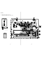
Page 23: ...ARDS PANEL Section See page 17 for Circuit Boards Location See page 18 for Note Semiconductor Location Ref No Location D801 B 3 D802 B 4 D803 B 1 IC801 D 5 IC802 E 7 Q801 B 3 Q811 C 3 Q812 B 4 Q813 B 2 27 28 Page 23 Page 20 Page 23 ...

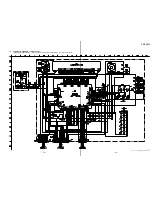
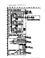
Page 24: ...CDP CX53 7 6 SCHEMATIC DIAGRAM PANEL Section See page 34 for Waveforms See page 41 for IC Pin Function Description See page 18 for Note 29 30 ...

Page 25: ... Page 23 7 7 PRINTED WIRING BOARDS SENSOR MOTOR Section See page 17 for Circuit Boards Location See page 18 for Note 31 Page 23 Page 23 ...

Page 26: ... 32 Page 32 Page 32 ...

Page 27: ... 33 7 8 SCHEMATIC DIAGRAM SENSOR MOTOR Section See page 18 for Note ...

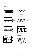
Page 28: ... 2 IC101 º FE PLAY MODE 3 IC101 7 TE PLAY MODE 4 IC102 PCK 5 IC102 XOUT 6 IC102 º 16M 7 IC102 4 2M PANEL Section 1 IC801 10MHz 1 6 Vp p 0 3 0 2 560 mVp p 460 mVp p 6 2 V 230 nsec 3 6 Vp p 16 9344 MHz 5 4 Vp p 4 2 MHz 4 4 Vp p 10 MHz 6 2 Vp p 16 MHz ...

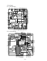
Page 29: ...XOUT XVDD MUTER RVDD RCHO RVSS LVSS LCHO LVDD MUTEL N C TEST4 TAI PDO VVSS ISET VVDD FR VSS EFMO EFMIN TEST2 CLV CLV V P HFL TES SLICE LEVEL CONTROL µCOM INTERFACE XTAL TIMING GENERATOR 2K x 8BIT RAM RAM ADDRESS GENERATOR MUTE SERVO COMMANDER CLV DIGITAL SERVO DIGITAL ATTENUATOR OVERSAMPLING DIGITAL FILTER 1BIT DAC L P F DIGITAL OUT GENERAL PORT VCO CLOCK OSCILLATION CLOCK CONTROL SYNCRONOUS DETEC...

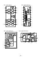
Page 30: ...IFT LEVEL SHIFT REGULATOR RESET Vcc 1 2 3 4 5 7 6 V IN EN GND CDEL CN RES V OUT REFERENCE VOLTAGE OVER HEAT PROTECTION OVER CURRENT LIMITTER ON OFF RESET GEN ERROR AMP VIN2 FIN2 RIN2 CT2 VEE FBIN FBIN OUT2 OUT2 VIN1 FIN1 REVERSIBLE DRIVER FWD REV CONTROLLER COVERNER DRIVER FWD REV CONTROLLER COVERNER LOAD CURRENT DETECTION AMPLIFIER COVERNER OUTPUT REFERENCE VOLTAGE OUTPUT LOW VOLTAGE OUTPUT RIN1 ...

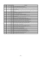
Page 31: ...ocusing phase compensation constant between FD pin and FA pin ª pins 19 FA I Creates a focusing phase compensation constant between FA pin and FE pin º pins 20 FE O Focus error signal output terminal 21 FE I Focus error signal invert signal input terminal 22 AGND Ground terminal analog system 23 SP O Single end output of the CV pin º and CV pin ª pins signal 24 SPI I Spindle amplifier input termin...

Page 32: ...and serial clock signal input from the system controller IC801 52 DAT I Command serial data input from the system controller IC801 53 CE I Command chip enable signal input from the system controller IC801 54 DRF O RF level detection signal output to the system controller IC801 55 FSS I FSS Focus Search Select is a switching terminal for the focus search mode search search for a reference voltage N...

Page 33: ...ock monitor output terminal 4 3218 MHz when phase is locked 22 FSEQ O Sync signal detection output terminal H when a sync signal detected from the EFM signal and that generated internally coincide 23 VDD Power supply terminal 5V digital system 24 CONT1 I Guard frame sync input terminal 25 CONT2 I Sled servo on off control signal input terminal 26 CONT3 O Sled servo drive control signal output term...

Page 34: ... Q synchronizing signal output to the system controller IC801 54 RWC I Command chip enable signal input from the system controller IC801 schmitt input 55 SQOUT O Subcode Q output to the system controller IC801 56 COIN I Command serial data input from the system controller IC801 57 CQCK I Command serial clock signal input from the system controller IC801 schmitt input Fetching clock input or subcod...

Page 35: ...80 IC601 L active 20 DOWN SW I Inputs the loading out switch S52 detection signal 21 UP SW I Inputs the loading in switch S51 detection signal 22 DSENS I Inputs the disc sensor Q51 detection signal A D input 23 KEY0 I Key input terminal A D input S801 802 and RE801 CLEAR CHECK DISC PUSH ENTER keys input 24 KEY1 I Key input terminal A D input S803 to 810 p P PLUS ONE REPEAT PLAY MODE keys input 25 ...

Page 36: ...erminal 5V 73 VDD Power supply terminal 5V 74 75 NC O Not used open 76 BUSOUT O Audio bus signal output for the audio bus interface 77 TEST PULSE O Table position detect pulse output terminal for disc sensor alignment 78 WRQ I Subcode Q synchronizing signal input from the DSP IC102 79 TSENS3 I Disc table home position detect sensor IC53 input terminal 80 TSENS2 I Disc table flag detect sensor IC52...

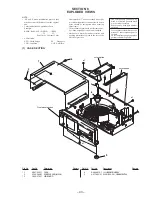
Page 37: ...d views are not supplied Hardware mark list and accessories and packing materials are given in the last of the electrical parts list NOTE XX and X mean standardized parts so they may have some difference from the original one Color Indication of Appearance Parts Example KNOB BALANCE WHITE RED Parts Color Cabinet s Color Ref No Part No Description Remark Ref No Part No Description Remark 1 CASE SEC...

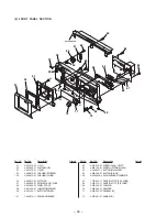
Page 38: ...OSE 56 4 989 312 01 LATCH NS 57 3 008 600 01 EMBLEM 5 AR SONY 58 4 997 062 01 PANEL FRONT 59 4 991 156 01 INDICATOR POWER 60 4 991 152 11 BUTTON POWER 61 1 668 574 11 POWER SW BOARD 62 4 951 620 01 SCREW 2 6X8 BVTP 63 4 933 134 61 SCREW PTPWH M2 6X6 64 X 4949 357 1 BUTTON MAIN ASSY 65 4 996 359 01 BUTTON BLOCK 66 A 4699 958 A DISPLAY BOARD COMPLETE 67 1 773 034 11 WIRE FLAT TYPE 15 CORE 68 1 765 3...

Page 39: ...7 4 997 124 51 PANEL BACK SP 108 1 558 943 41 CORD POWER E 108 1 575 651 21 CORD POWER AEP AED SP 108 1 590 926 11 CORD POWER US CND 108 1 696 845 11 CORD POWER AUS 109 1 569 007 11 ADAPTOR CONVERSION 2P E 110 4 966 266 01 BUSHING S FBS002 CORD E 110 4 966 267 11 BUSHING FBS001 CORD EXCEPT E 111 1 783 171 11 WIRE FLAT TYPE 12 CORE 112 4 990 029 01 RING B 113 X 3371 435 1 FOOT SMALL ASSY 114 4 978 ...

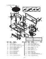
Page 40: ...020 1 LEVER LOADING ASSY 309 4 988 438 01 SPRING LEVER TENSION 310 4 988 437 01 SPRING HOLDER TORSION 311 4 988 416 01 BASE LOADING 312 4 988 419 01 HOLDER B DISC 313 4 992 069 01 SCREW PTPWH M2 DIA 7 314 4 988 454 01 COVER LEVER 315 4 988 421 01 HOLDER MAGNET 316 A 4672 522 A MAGNET ASSY 317 4 960 633 11 YOKE MAGNET 318 4 999 139 01 PULLEY B 319 4 976 473 01 HOLDER LED S 320 4 988 431 01 ROLLER D...

Page 41: ...62 351 1 663 971 11 TABLE SENSOR BOARD 352 4 988 414 01 BELT 353 4 988 423 01 GEAR A LOADING 354 4 988 425 01 PULLEY 355 4 988 424 01 GEAR TABLE 356 4 988 432 01 GEAR B LOADING 357 4 988 426 01 BASE CDM 358 1 663 972 11 DISC SENSOR R BOARD 359 1 663 974 11 CD MOTOR BOARD 360 4 990 669 01 HOLDER SENSOR M61 X 4948 434 1 MOTOR ASSY LOADING M62 X 4948 434 1 MOTOR ASSY TABLE ...

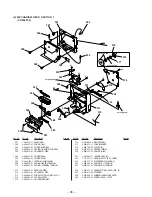
Page 42: ...T SLED 405 A 4699 968 A BD BOARD COMPLETE 406 4 992 054 01 RUBBER VIBRATION PROOF 407 4 996 243 01 SCREW M2 PSW 408 1 777 874 11 WIRE FLAT TYPE 16 CORE M101 X 2646 110 1 T T CHASSIS ASSY MG F SPINDLE M102 X 2625 769 1 MOTMR GEAR ASSY MB RP SLED The components identified by mark or dotted line with mark are critical for safety Replace only with part num ber specified Les composants identifiés par u...

Page 43: ... 20 10V C507 1 161 494 00 CERAMIC 0 022uF 25V C511 1 161 494 00 CERAMIC 0 022uF 25V C701 1 126 936 11 ELECT 3300uF 20 16V C702 1 126 767 11 ELECT 1000uF 20 16V C703 1 126 968 11 ELECT 100uF 20 50V C704 1 126 965 11 ELECT 22uF 20 50V C706 1 126 963 11 ELECT 4 7uF 20 50V C707 1 126 963 11 ELECT 4 7uF 20 50V C708 1 126 935 11 ELECT 470uF 20 6 3V C709 1 126 963 11 ELECT 4 7uF 20 50V C710 1 126 934 11 ...

Page 44: ...1 4W R606 1 249 428 11 CARBON 8 2K 5 1 4W R701 1 249 425 11 CARBON 4 7K 5 1 4W R704 1 249 431 11 CARBON 15K 5 1 4W R705 1 249 429 11 CARBON 10K 5 1 4W R706 1 249 411 11 CARBON 330 5 1 4W R851 1 249 429 11 CARBON 10K 5 1 4W R852 1 249 425 11 CARBON 4 7K 5 1 4W R853 1 249 429 11 CARBON 10K 5 1 4W R854 1 249 393 11 CARBON 10 5 1 4W VARIABLE RESISTOR RV502 1 241 768 11 RES ADJ CARBON 220K SWITCH S501 ...

Page 45: ...7 00 RES CHIP 100K 5 1 10W R107 1 216 097 00 RES CHIP 100K 5 1 10W R108 1 216 068 00 METAL CHIP 6 2K 5 1 10W R109 1 216 076 00 METAL CHIP 13K 5 1 10W R110 1 216 093 00 METAL CHIP 68K 5 1 10W R111 1 216 057 00 METAL CHIP 2 2K 5 1 10W R112 1 216 109 00 METAL CHIP 330K 5 1 10W R113 1 216 099 00 METAL CHIP 120K 5 1 10W R114 1 216 055 00 METAL CHIP 1 8K 5 1 10W R115 1 216 689 11 METAL CHIP 39K 0 5 1 10...

Page 46: ...ICATOR TUBE FLUORESCENT IC IC801 8 752 891 31 IC CXP82324 088Q IC802 8 749 014 66 IC NJL56H400 TRANSISTOR Q801 8 729 119 76 TRANSISTOR 2SA1175 HFE Q811 8 729 029 66 TRANSISTOR DTC114ESA Q812 8 729 029 66 TRANSISTOR DTC114ESA Q813 8 729 029 66 TRANSISTOR DTC114ESA RESISTOR R800 1 249 427 11 CARBON 6 8K 5 1 4W R801 1 249 415 11 CARBON 680 5 1 4W R802 1 249 417 11 CARBON 1K 5 1 4W R803 1 249 427 11 C...

Page 47: ...408 11 CARBON 180 5 1 4W 1 663 974 11 MOTOR BOARD CONNECTOR CN61 1 506 469 11 PIN CONNECTOR 4P 1 668 574 11 POWER SW BOARD CONNECTOR CN802 1 568 942 11 PIN CONNECTOR 4P LED D804 8 719 057 09 LED LNJ801LPDJA STANDBY TRANSISTOR Q814 8 729 029 66 TRANSISTOR DTC114ESA RESISTOR R844 1 249 407 11 CARBON 150 5 1 4W R845 1 249 417 11 CARBON 1K 5 1 4W SWITCH S816 1 554 303 21 SWITCH TACTILE I u 1 663 975 1...

Page 48: ... 3 862 222 31 MANUAL INSTRUCTION GERMAN DUTCH ITALIAN PORTUGUESE AEP 3 862 222 41 MANUAL INSTRUCTION SWEDISH DANISH FINNISH AED 4 981 643 01 COVER BATTERY for RM DX53 4 991 161 01 LET 50 BOOK 4 991 854 01 LABEL DISC HARDWARE LIST 1 7 685 871 01 SCREW BVTT 3X6 S 2 7 685 534 19 SCREW BTP 2 6X8 TYPE2 N S 3 7 685 646 79 SCREW BVTP 3X8 TYPE2 N S 4 7 685 872 09 SCREW BVTT 3X8 S 5 7 685 647 79 SCREW BVTP...

Reviews: