background image

XE-A212V

HARDWARE DESCRIPTION

– 7 –

3. PRINTER CONTROL

3-1. STEPPING MOTOR CONTROL

The two phase Bi-Polar stepping motor is driven at a constant voltage 

by SANYO LB1838M.

1step: 0.087mm, 1dot: 2step

< CPU’s PORT >

< Driving steps >

*

When the motor is at rest, the same phase as the final excitation

phase is RUSH energize to turn off all phases. 

3

 Turn ENA1 and

ENA2 into L.

No energizing should be allowed at lease 40 ms after stopping the
motor before restarting.

When starting the motor etc, required the chopping

3-2. HEAD CONTROL

HEAD:

288 dots in all,  width: 0.167mm/dot (6dot/mm)

<Related PORT>

Conduction pulse width: Refer to the M-T53

II

 specifications.

*

When turning on or off the printer power supply, make sure to turn

/STB1, 2 to “H”.

*

Do not turn on without paper.

*

THERMAL HEAD power supply control : Turns ON when P105= “H”;
turns OFF when “L”. (The power supply for HEAD and STEPPING

MOTOR is shared). When printing is finished (when the motor is

stopped) Athe power should be turned OFF.

*

Before printing or feeding paper, perform A/D conversion in 20 ms
after the printer head is turned ON and make sure the voltage is sta-

ble.

(The power supply of the printer head should be turned ON and OFF
by using the regulator IC.)

*

The head rank confirmation was abolished.

3-3. WINDING MOTOR CONTROL

<Related port>

3-4. PAPER EMPTY DETECTION

When LOW is detected twice continuously in sampling of signals for

every one dot line, it is judged as paper empty. 

The threshold level of High/Low level is 2.5 

m

 0.2V. (Vcc = 5VDC 

m

 5%)

When paper empty is detected, printing is terminated. However, when
paper empty is detected during printing, 15-dot lines from detection of

paper empty can be printed.

3-5. PLATEN OVER

When signals are sampled in the frequency of 1ms or less and open

state is detected twice continuously, it is judged as platen over. 

If the head is conducted under the platen over state, the thermal head
life may be shortened. When, therefore, platen over is detected, printing

is terminated.

Under the platen over state (switch open state), driving the paper feed

motor is inhibited.

No.

CPU PORT

Signal to be used

76

P14

IN1

75

P15

IN2

74

P16

ENA1

73

P17

ENA2

Driver IC input

(CPU output)

Motor driving signal

STEP

IN1

IN2

ENA1

ENA2

A

(OUT1)

B

(OUT3)

/A

(OUT2)

/B

(OUT4)

1

L

L

H

H

H

H

L

L

2

H

L

H

H

L

H

H

L

3

H

H

H

H

L

L

H

H

4

L

H

H

H

H

L

L

H

No.

I/O

PORT

Function

Signal

name

Initial 

value

Port setup 

in single 

chip mode

18

OUT

P84

PRINTING

/STB2

H

Out L

89

OUT

P107

PRINTING

/STB1

H

Out L

30

OUT

P70

TXD2

PRINTING

DAT

(Print DATA)

H

Out L

28

OUT

P72

CLK2

PRINTING

PCLK

(Transfer Clock)

Out L

90

OUT

P106

PRINTING

/LAT

(DATA Latch)

H

Out L

91

OUT

P105

PRINTING

VPON (Head 

motor POWER 

SUPPLY)

L

Out L

/STB1: 1 ~ 144 dot: 144 dots in all

Total 288 dots

/STB2: 145 ~ 288 dot: 144 dots in all

OFF time of print strobe

: Conduction strobe OFF time between dots

min. 160us

Logo print ratio restriction : Average print ratio 35% or below (Same as

the M-T51)
When the print ratio at the peak one-dot

line is 50%, the average print ratio of 10-

dot line including the above line should be
35% or less.

No. I/O

PORT Function

Signal

name

Initial
value

Port setup in

single chip mode 

21 Out

P81

Printer motor

(Winding motor)

L

ON

Summary of Contents for XE-A212

Page 1: ...published to be used for after sales service only The contents are subject to change without notice XEA212VSME ELECTRONIC CASH REGISTER MODEL XE A212 V version CHAPTER 1 SPECIFICATIONS 1 CHAPTER 2 OPTIONS 5 CHAPTER 3 MASTER RESET AND PROGRAM RESET 5 CHAPTER 4 HARDWARE DESCRIPTION 6 CHAPTER 5 DIAGNOSTIC PROGRAM 12 CHAPTER 6 IPL FROM EP ROM 16 CHAPTER 7 CAUTION TO BE USED WHEN CONNECTING THE RS 232 ...

Page 2: ... cradle Paper positioning guides 7 6 5 4 3 2 1 14 13 12 11 10 9 8 21 20 19 18 17 16 15 28 27 26 25 24 23 22 35 34 33 32 31 30 29 42 41 40 39 38 37 36 49 48 47 46 45 44 43 56 55 54 53 52 51 50 63 62 61 60 59 58 57 70 69 68 67 66 65 64 1 2 3 4 5 6 0 1 2 3 4 5 6 7 8 9 CL 00 GC RCPT ESC RCPT EX VAT PO RA RF NS ST TL CH1 CH2 CR1 CR2 GLU NBAL DEPT L1 AUTO L2 L3 CLK SUB PLU KEY TOP DESCRIPTION 2 Paper fe...

Page 3: ... an amount is to be entered is displayed at the numeric entry area with AMOUNT When a preset price has been set the price is displayed at the numeric entry area with AMOUNT Numeric entry display area Numbers entered using numeric keys are displayed here Date and time display Date and time appear on the display in the OP X Z REG or MGR mode In the REG or MGR mode press the key to display the date a...

Page 4: ... additional drawers 0 The drawer consists of 1 Drawer box outer case and drawer 2 Money case 3 Lock attached to the drawer SPECIFICATION 1 DRAWER BOX AND DRAWER 2 MONEY CASE Layout 3 LOCK LOCK KEY LKGIM7331BHZZ Location of the lock Front Method of locking and unlocking To lock insert the drawer lock key into the lock and turn it 90 degrees counter clockwise To unlock insert the drawer lock key and...

Page 5: ... numeric entry any item entry is not done or just after finalization The machine can indicate the low battery condition Always CASE 2 When numeric entry or item entry is done Battery condition will not appear Exceptionally when the power is restored after a power failure the low battery condition will appear on the display only when the bat tery is low And the indicator will disappear after any ke...

Page 6: ...ormed after the power has been restored This is because if power failure occurs with no battery attached to the machine all the memories are lost and the machine does not work properly after power recovery this requires the master reset operation 2 PROGRAM RESETTING INITIALIZATION This resetting resumes the initial program without clearing memory This resetting can be operated at below sequence in...

Page 7: ...B x 2 FLASH ROM CS0 area BANK 0 address 80000h FFFFFh 256KB Moves to Bank 1 when rewritten using EPROM Reserve CS0 area BANK 6 address 80000h FFFFFh 256KB I O CS3 area BANK 0 address 04000h 07FFFh 16KB 00000h 00400h 02C00h 04000h 08000h 28000h 30000h 40000h 60000h 80000h C0000h FFFFFh Bank 0 Bank 1 Bank 2 Bank 3 Bank 4 Bank 5 Bank 6 Bank 7 BR1 0 0 1 1 0 1 1 0 BR2 1 1 1 1 0 0 0 0 BR0 1 1 0 1 0 1 0 ...

Page 8: ...Vcc 5VDC m 5 When paper empty is detected printing is terminated However when paper empty is detected during printing 15 dot lines from detection of paper empty can be printed 3 5 PLATEN OVER When signals are sampled in the frequency of 1ms or less and open state is detected twice continuously it is judged as platen over If the head is conducted under the platen over state the thermal head life ma...

Page 9: ...A2 P73 27 O P73 DRAWER 1 L Out L DRAWER DRIVE SIGNAL P20 72 O A0 A0 Out L P74 26 O P74 ER1 H Out L RS 232 ER1 P21 71 O A1 A1 Out L P75 25 I P75 CD1 In RS 232 CD1 P22 70 O A2 A2 Out L P76 24 I P76 CS1 In RS 232 CS1 P23 69 O A3 A3 Out L P77 23 I P77 DR1 In RS 232 DR1 P24 68 O A4 A4 Out L P80 22 O P80 BUZZER L Out L P25 67 O A5 A5 Out L P81 21 O P81 MOTOR L In Printer winding motor P26 66 O A6 A6 Out...

Page 10: ... Keyboard 04001h 04003h PORT PIN No I O Pin name Function PORT PIN No I O Pin name Function BYTE 8 I BYTE Connected to VDD Vcc 62 Vcc Connected to VDD CNVss 9 I CNVss Connected to VDD Vss 64 Vss connected to GND RESET 12 I RESET AVss 96 AVss Connected to GND Xout 13 O Xout OPEN Vref 98 Vref Connected to VDD Vss 14 Vss Connected to GND AVcc 99 AVcc Connected to VDD Xin 15 I Xin connected to Spectra...

Page 11: ...om COM Data from the PC is written to flash ROM through the COM port Max 38 4 kbps 8 DRAWER The machine has a 1 channel of drawer port No open sensor is provided The driving time for the DRAWER solenoid are as follows 50ms max 45ms min CPU STO ST1 ST2 ST3 ST4 ST5 ST6 ST7 ST8 ST9 MODE P90 SRV PGM Time REG MGR X1 Z1 X2 Z2 KEYBD Others P91 PF HEAD UP PE DRAWER OPEN RS 232 CI1 KEYBD 1 Normal Keyboard ...

Page 12: ...ltage The RESET signal is generated under the following conditions 1 When the mode key switch is set from SRV to another position except for OFF position 2 When the power is turned on after 5sec or more from turning off the power and the VCC reaches 5V 3 When the mode key switch is set from OFF position to another posi tion except for SRV position and VCC reaches 5V If the OFF time is within 5sec ...

Page 13: ...2 KEY CODE 1 Key operation 101 3 2 Test procedure 3 Check 4 End of testing You can exit the test mode by turning the mode switch to a position other than the PGM mode The printer prints as follows 1 0 1 Code Description 1 100 Display buzzer test 2 101 Key code 3 102 Printer test 4 104 Keyboard test 5 105 Mode switch test 6 106 Printer sensor test 7 107 Clock display test 8 110 Drawer 1 open sensor...

Page 14: ...ed when DIAG is started 5 MODE SWITCH TEST 1 Key operation 105 3 2 Test procedure The above X must be read in the correct order If the contact is open 9 will be displayed 3 Check The display during testing and the content of the completion print 4 End of testing 6 PRINTER SENSOR TEST 1 Key operation 106 3 2 Test procedure Check the status of the paper end sensor and head up sensor 3 Check the foll...

Page 15: ...ng The program ends after printing as follows When an error occurs the printer outputs the error message and the address where the error has occurred in the area 10 CPU INTERNAL RAM TEST 1 Key operation 121 3 2 Test procedure The test program tests internal RAM 10 Kbytes of the CPU The contents of memory must be stored before and after this test RAM 00400H 02BFFH area is tested in the following pr...

Page 16: ...nds abnormally E 1 3 0 ROM Model name Version PO R O M F L A S H P G M OP display 1 3 0 PO T M P G M OP display Display 1 6 0 V R F P G M OP display 1 6 0 V P T E S T P G M OP display 1 6 0 End of testing OUTPUT INPUT ER RS DR CI CD CS OFF OFF OFF OFF OFF OFF OFF ON OFF OFF ON ON ON OFF ON ON OFF OFF ON ON ON ON ON ON Completion print RS TEST OK 500 Error print RS TEST NG ERxx 500 xx Contents of e...

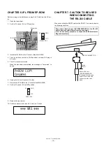
Page 17: ...et of the MAIN PWB 8 Set the IPL switch S1 to GND position 9 Replace the top cabinet 10 Perform a master reset insert AC cord in AC outlet CHAPTER 7 CAUTION TO BE USED WHEN CONNECTING THE RS 232 CABLE When connecting the RS 232 cable to the XE A212 be sure to observe the following condiiton IPL switch IPL ROM 1pin GND VCC S1 ROM COPY P ROM COPY Completed GND VCC S1 ROM COPY MRS Secure the attached...

Page 18: ... 15 16 17 18 19 20 21 22 23 24 25 26 27 28 29 30 79 78 77 76 75 74 73 72 71 70 69 68 67 66 65 64 63 62 61 60 59 58 57 56 55 54 53 52 51 50 49 48 47 46 45 44 43 42 41 40 39 38 37 36 35 34 33 32 31 D7 D8 D6 D5 D4 D3 D2 D1 D0 AN7 AN6 AN5 AN4 AN3 AN2 AN1 AVSS AN0 VREF AVCC SIN4 SOUT4 CLK4 TB4IN TB3IN SOUT3 SIN3 CLK3 BYTE CNVSS XCIN XCOUT RESET XOUT VSS XIN VCC NMI INT2 INT1 INT0 TA4IN U TA4OUT U TB3IN...

Page 19: ... Q4 LE C83 0 1uF Q3 KRC111S B E C R94 10K CN4 R LCD CN 1 2 3 4 5 6 IC14 74HC273 3 4 7 8 13 14 17 18 11 1 2 5 6 9 12 15 16 19 D1 D2 D3 D4 D5 D6 D7 D8 CLK CLR Q1 Q2 Q3 Q4 Q5 Q6 Q7 Q8 FB3 JUMPER C134 10uF 16V C66 0 1uF C67 0 1uF CN6 DR CN 2Pin 5046 03A 1 2 3 IC17 BA00ASFP 2 1 4 5 6 3 R99 12K D21 1SS355 A K Q2 2SD2212 B E C C82 0 1uF R96 5 6K R100 10K IC21 74HC245 1 2 3 4 5 6 7 9 10 8 20 19 18 17 15 1...

Page 20: ...5 A K R167 0 R116 4 7K C87 10u F 50V R19 1K Q6 2SK2731 G D S CN12 PRINTER CN 1 2 3 4 5 6 7 8 9 10 11 12 13 14 15 16 17 18 19 20 21 22 23 24 25 26 R111 20K R114 10K Q8 KRC111S B E C C86 0 1uF Q7 2SK2731 G D S C91 10u F 50V C88 47uF 50V C85 0 1uF R112 10K D6 1SS355 A K CN7 MO TOR CN 1 2 D18 1SS355 A K R115 30KF C133 22u F 16V FB5 0 EFCB322513TS R109 47K Q4 2SD2212 B E C IC22 LB1838M 1 2 13 6 9 7 14 ...

Page 21: ...P2 VBAT2 1 R133 100 CN9 Mn B AT CN 1 2 D7 FMB G24H A K R141 10K PS CN 1 2 R143 560 IC25A BA10393F 3 2 1 8 4 R119 18 0KF Q12 KRC106S B E C ZD4 UDZ5 1B A K D13 RB551 30 A K R134 1KF R127 3KF Q11 KRA106 S B E C R136 3 9K CN8 PS CN 1 2 TP1 VO 1 R132 220 R122 5 6K L2 180uH Ch ock POWER TRANS3 100V 50 Hz 60Hz F5 T2 0A 250V R142 6 2KF D12 1SR159 200 A K R118 10 FUSE R R120 3 3KF R139 56K ZD3 UDZ5 1B A K ...

Page 22: ...TK A 1 2 3 4 5 6 7 8 9 10 11 12 13 14 15 16 17 18 19 20 21 22 23 24 25 26 CN31 JST 27FMN B YK A 1 2 3 4 5 6 7 8 9 10 11 12 13 14 15 16 17 18 19 20 21 22 23 24 25 26 27 A B C D 8 7 6 5 4 3 2 1 1 2 3 4 5 6 7 8 D C B A A B C D 8 7 6 5 4 3 2 1 1 2 3 4 5 6 7 8 D C B A A B C D 8 7 6 5 4 3 2 1 1 2 3 4 5 6 7 8 D C B A A B C D 8 7 6 5 4 3 2 1 1 2 3 4 5 6 7 8 D C B A 6 7 M T53II Printer I F ...

Page 23: ...0 0 1uF IC27 HIN211 12 14 15 16 7 6 20 21 8 5 26 22 19 24 13 17 2 3 1 28 9 4 27 23 18 25 11 10 C1 C1 C2 C2 T1IN T2IN T3IN T4IN R1OUT R2OUT R3OUT R4OUT R5OUT EN V V T1OUT T2OUT T3OUT T4OUT R1IN R2IN R3IN R4IN R5IN SHDN VCC 10 R155 10K R156 10K R157 10K FB9 R158 10K F7 T500mA 250 V R151 C119 1000pF R160 10K FB10 FB7 FB11 FB8 C115 0 1uF R150 FB12 C113 10u F 50V SP1 1 3 2 R152 R153 C120 1000pF FB13 D1...

Page 24: ...XE A212V CIRCUIT DIAGRAM AND PWB LAYOUT 23 PWB LAYOUT MAIN PWB LAYOUT A side ...

Page 25: ...XE A212V CIRCUIT DIAGRAM AND PWB LAYOUT 24 B side ...

Page 26: ...MEMO ...

Page 27: ......

Page 28: ...03 August Printed in Japan t COPYRIGHT 2003 BY SHARP CORPORATION All rights reserved Printed in Japan No part of this publication may be reproduced stored in a retrieval system or transmitted In any form or by any means electronic mechanical photocopying recording or otherwise without prior written permission of the publisher ...

Reviews: