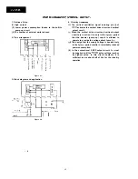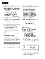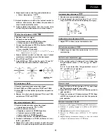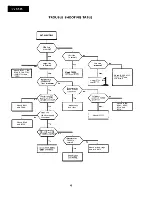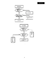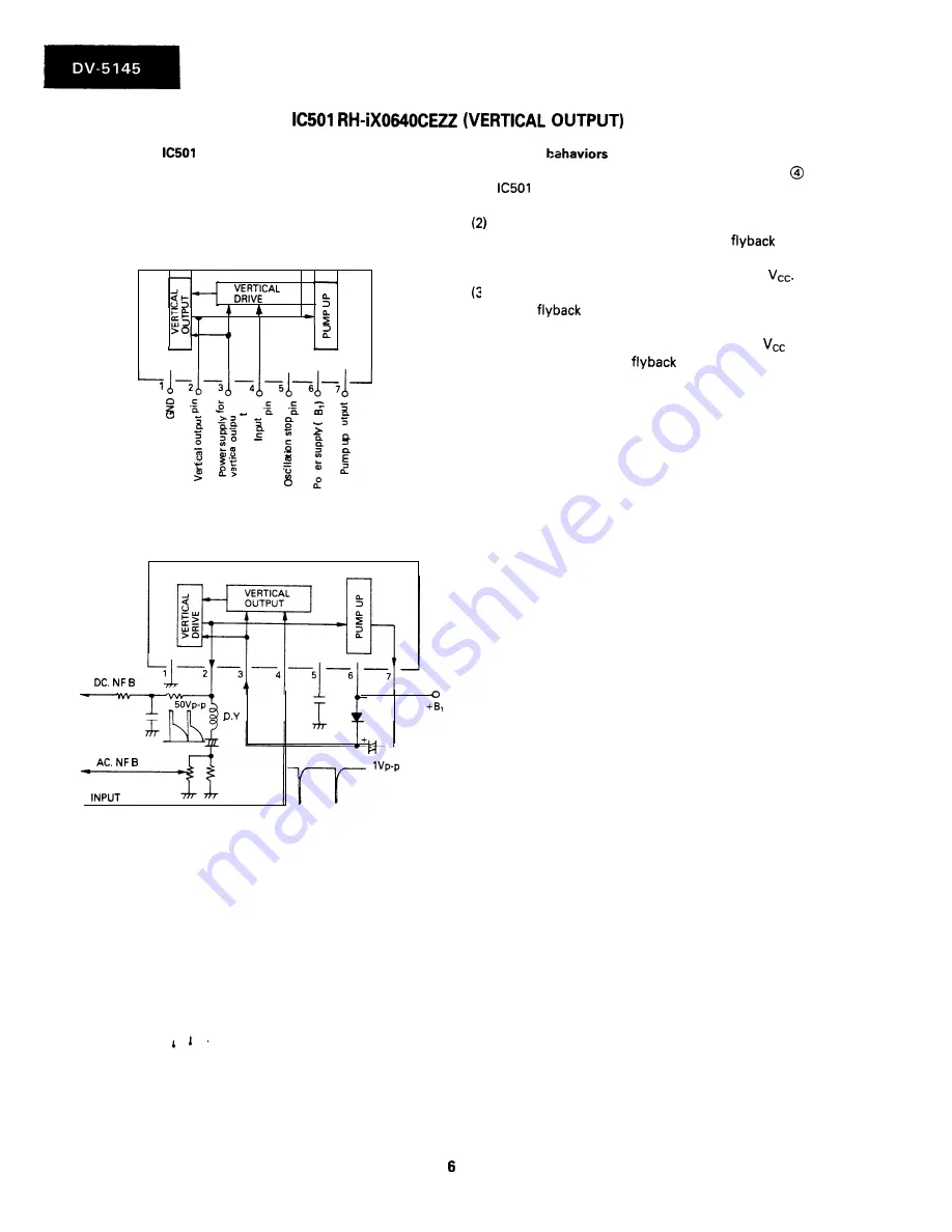
1. Outline of
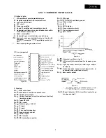
(I) High output
(2) Lower power consumption thanks to the built-in
4. Circuitry
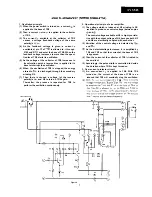
(I) The vertical oscillation signal entering pin
of
pump up circuit
(3) The number of external parts reduced
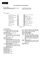
2. Pins arrangement
,
+
0
3
activates the vertical drive circuit and vertical
output circuit.
When the vertical drive circuit and vertical output
circuit are in action, it is only in the
period
that the booster (pump up) circuit is allowed to
operate to provide the voltage about twice
I) The design that the supply voltage is boosted only
in the
period results in remarkably reduced
power consumption.
(4) In the conventional SRPP output circuit,
must
be supplied until the
pulse voltage reaches
its highest value. In this circuit, however, it is
sufficient to use about half of Vcc for the circuitry
operation.
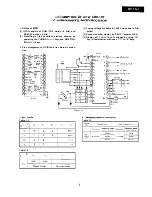
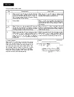
Figure 3-1.
3. Block diagram and application
Figure 3-2.
Summary of Contents for DV-5145
Page 32: ...S H A R P T5157 S MW KY ...


