background image

Ref. No.

Part No.

Description

Code

Ref. No.

Part No.

Description

Code

48

CX51N3/N4

SHARP CORPORATION
AV Systems Group
Quality & Reliability Control Center
Yaita, Tochigi 329-2193, Japan

COPYRIGHT  

©

  2002 BY SHARP CORPORATION

ALL RIGHTS RESERVED.

No part of this publication may be reproduced,

stored in a retrieval system, or transmitted in

any form or by any means, electronic, mechanical,

photocopying, recording, or otherwise, without

prior written permission of the publisher.

D SEM   P SREC  TQ1417-S
OCT. 2002 Printed in JAPAN

MY. KY

Summary of Contents for CX51N3

Page 1: ...BASE DIAGRAM 18 WAVEFORMS 19 CHASSIS LAYOUT 20 BLOCK DIAGRAM 22 DESCRIPTION OF SCHEMATIC DIAGRAM 26 SCHEMATIC DIAGRAM Ë CRT UNIT 27 Ë MAIN UNIT 28 Page Ë HEADPHONE UNIT 32 Ë BURST UNIT 33 PRINTED WIRING BOARD ASSEMBLIES 34 REPLACEMENT PARTS LIST Ë ELECTRICAL PARTS MAIN UNIT 40 CRT UNIT 43 HEADPHONE UNIT 43 BURST UNIT 44 Ë SUPPLIED ACCESSORIES 44 Ë PACKING PARTS 44 Ë CABINET PARTS 44 Ë CABINET PART...

Page 2: ...1 Picture tube in this receiver employs integral implosion protection 2 Replace with tube of the same type number for continued safety 3 Do not lift picture tube by the neck 4 Handle the picture tube only when wearing shatterproof goggles and after discharging the high voltage completely X RAY This receiver is designed so that any X Ray radiation is kept to an absolute minimum Since certain malfun...

Page 3: ...ata Note Once the chassis has been assembly together and ready to be POWER ON for the FIRST TIME make sure to make a short circuit 137 and 138 switch to the service mode position first and then turn on the main power switch See 2 1 above Precaution If haven t done this initiation it may possibly generate excessive Beam current 3 For reference please check with memory map GA1 Series type RH iX3368C...

Page 4: ...CK SECAM P SECAM FE RF NTSC 3 58 F N358 FE RF NTSC 4 43 F N443 FE RF SECAM F SECAM VIDEO MUTE AT IDENT LOSS VMI VIDEO MUTE AT PROGRAM SOURCE CHANGE VMC HOTEL MODE HTL REDUCED FM DEMODULATION GAIN FOR BTSC SIGNAL BTSC A A NUMBER OF EXT AV SOURCE AV FM WINDOW SELECTION FMWS SOUND MUTE BIT 0 SM0 SOUND MUTE BIT 1 SM1 THAI LANGUAGE THA ARABIC LANGUAGE ARA MALAY LANGUAGE MAL CHINESE LANGUAGE CHI FRENCH ...

Page 5: ...T SPECIFIC INSTRUCTION Please set the EEPROM initial data according to the value in parenthesis before adjustment 2 2 ADJUST COLOUR OFFSET AFTER ADJUST SUB COLOUR COLOUR OFFSET PAL COL OP 8 14 COLOUR OFFSET NTSC358 COL 03 4 10 COLOUR OFFSET NTSC443 COL 04 4 10 3 3 SET S DK 1 _ 0 S I 1 _ 0 P SECAM 1 _ 0 F N443 1 _ 0 F SECAM 1 _ 0 EEPROM ITEMS OSD DATA LENGTH INITIAL DATA FIX ADJ REMARK SHARPNESS OF...

Page 6: ... 41 10 42 41 10 43 41 10 44 174 95 B G 45 175 55 B G 46 41 10 99 41 10 INITIAL SETTING 1 Please set to MCL2 2 After set the MCL Please set the Initial setting to Initial 3 All channel Sound System will set to B G SHIPPING SETTING CHECKING 1 The following default data has been factory set for the E2 PROM ITEMS DATA SETTING LAST PROGRAM CHANNEL 1 FLASHBACK PROGARM CH 1 DIGIT 1 C SYSTEM AUTO S SYSTEM...

Page 7: ... RF AGC to 0 6 V with no saturation with the waveform 6 Adjust the tuner IF coil to obtain the waveform as shown in Fig 2 Note Be sure to keep the tuner cover in position during this adjustment E 9 CH P C 10k 100k 1n60 75ohm IF OUT 1 5 0 8dB 1000p Oscilloscope Fig 2 Fig 3 PURITY ADJUSTMENT NO Adjustment part Adjusting procedure and conditions Waveform and others 1 PURITY ADJ 1 Receive the GREEN ON...

Page 8: ... variable resistor until screen retrace line cut off Not Raster Note Must confirm the AKB function in set before continue the next adjustment CRT CUT OFF BACKGROUND AND SUB CONTRAST ADJUSTMENT NO Adjustment part Adjusting procedure and conditions Waveform and others 1 2 SUB BRIGHTNESS ADJUSTMENT I2 C BUS CONTROL Line 3 is one step data brighter than line 2 CRT CUTOFF ADJUSTMENT I2 C BUS CONTROL 3 ...

Page 9: ...OMA ADJUSTMENT NO Adjustment part Adjusting procedure and conditions Waveform and others 1 SUB TINT I2 C BUS CONTROL 1 Receive the NTSC3 58 Colour Bar signal thru AV in 2 Connect the oscilloscope to TP47B P882 pin 5 BLUE OUT Range 100mV div AC Use Probe 10 1 Sweep time 10 µsec div 3 Call the SUB TINT mode in service mode Adjust the SUB TINT bus data to obtain the waveform shown as Fig 1 1 4 Clear ...

Page 10: ...tting value for every mode CONTRAST MAX COLOUR CENTER BRIGHTNESS CENTER TINT CENTER SHARPNESS CENTER Note If nothing is display mean contrast colour bright tint or sharpness are all in nor mal setting 8 White Temp 1 Receive Monoscope Pattern signal 2 Set FUNCTION to select WHITE TEMP 3 Press Volume Up Down key to check WHITE TEMP Option STANDARD NORMAL SETTING WARM for more REDDISH direction chang...

Page 11: ...F 00 FF 2A 2B 2C 2D OSD REFERENCE 0F 00 0F 2E CUTOFF LEVEL OFFSET R 20 00 3F 2F CUTOFF LEVEL OFFSET G 20 00 3F 30 CATHODE DRIVE LEVEL 00 00 0F 31 Y DELAY TV PAL 0C 00 0F 32 Y DELAY TV SECAM 0F 00 0F 33 Y DELAY TV N358 0C 00 0F 34 Y DELAY TV N443 0C 00 0F 35 Y DELAY TV BW 0C 00 0F 36 Y DELAY AV PAL 0C 00 0F 37 Y DELAY AV SECAM 0F 00 0F 38 Y DELAY AV N358 0C 00 0F 39 Y DELAY AV N443 0C 00 0F 3A Y DE...

Page 12: ...ECK DATA CHECK TYPE REMARK ADDRESS DATA HEX D7 D6 D5 D4 D3 D2 D1 D0 40 SHARPNESS OFFSET SECAM 04 00 0F 41 SHARPNESS OFFSET N358 0C 00 0F 42 SHARPNESS OFFSET N443 08 00 0F 43 44 FCO ACL OSO EHT EVG FFI AVL BKS 00 FF 45 SECAM N443 N358 PB SECAM BG I DK M 00 FF 46 SM1 SM0 FMWS AV BTSC HTL VMC VMI 00 FF 47 HP2 FSL RUS FRA CHN MLY ARB THA 00 FF 48 AGC1 AGC0 BIL CPT FOB AV FOA AV FOB FE FOA FE NDF MSA L...

Page 13: ...O MICON EEPROM EEPROM CHASSIS CTV FINAL LAST INITIAL SETTING DATA DEFAULT RANGE WRITE CPU CHECK DATA CHECK TYPE CHECK DATA CHECK TYPE REMARK ADDRESS DATA HEX D7 D6 D5 D4 D3 D2 D1 D0 C0 TUNING FREQUANCY LOWER PART POS 25 C1 S SYS AFT auto C SYS C2 TUNING FREQUANCY HIGHER PART POS 26 C3 TUNING FREQUANCY LOWER PART C4 S SYS AFT auto C SYS C5 TUNING FREQUANCY HIGHER PART POS 27 C6 TUNING FREQUANCY LOW...

Page 14: ...S 149 TUNING FREQUANCY HIGHER PART POS 71 14A TUNING FREQUANCY LOWER PART 14B S SYS AFT auto C SYS 14C TUNING FREQUANCY HIGHER PART POS 72 14D TUNING FREQUANCY LOWER PART 14E S SYS AFT auto C SYS 14F TUNING FREQUANCY HIGHER PART POS 73 150 TUNING FREQUANCY LOWER PART 151 S SYS AFT auto C SYS 152 TUNING FREQUANCY HIGHER PART POS 74 153 TUNING FREQUANCY LOWER PART 154 S SYS AFT auto C SYS 155 TUNING...

Page 15: ...ll be the last ch which you received before power off same as normal operation CONDITION When using hotel mode user can control contrast brightness sharpness and tint function But after power off it will return to the initial setting You can t use Preset mode Fine tuning Skip mode System selection The others function is allowed to be used 1 Ch 1 is your selected channel for hotel mode Input 1 3 7 ...

Page 16: ...eived Check the tuner supply voltage LB must be approx 5V BT must be approx 32V and CH preset data check Check the tuner AGC at TP201 Does noise or signal appear at pin 38 of IC801 Check IC801 and its related circuit Check pin 1 of SF201 Tuner and related circuit Check pin 37 of IC801 and related circuit Check Q253 Q254 and related circuit Check IC801 Check C356 and peripheral circuit Check pin 27...

Page 17: ... R501 R521 R503 R512 R533 and C533 TROUBLE SHOOTING TABLE Continued NO SPECIFIC COLOUR Is some colour produced in B W broadcast reception Is the white balance properly adjusted Readjust the white balance The picture colour is yellow The picture colour is magenta The picture colour is cyan Check Q870 Q885 and its adjacent circuits Check Q871 Q883 and its adjacent circuits Check Q872 Q887 and its ad...

Page 18: ...2 TX0110BM TX0124BM 2SC3207 2PC1815 DX0476CE BASE COLLECTOR EMITTER BASE COLLECTOR EMITTER B C E KA7808A 1 2 3 CATHODE ANODE RED STRG5653 AN7523 PX0013PE 2SD2586 C4S584F 1 9 ZR BR COLLECTOR COLLECTOR BASE EMITTER BASE EMITTER JC COLLECTOR BASE EMITTER 1 3 5 2 4 9 TDA9302 IX3368CE 2SC2735 1 32 5 VDD NC OUT Y IN Y VSS 4 1 3 2 ...

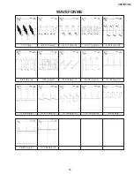
Page 19: ... 3 11 Vp p H 4 3 11 Vp p H 5 84 8 Vp p H 2 3 17 Vp p H 6 80 Vp p H 8 3 04 Vp p V 9 2 28 Vp p H 10 126 Vp p H 7 80 Vp p H 11 8 8 Vp p H 13 146 Vp p H 14 1 1kVp p H 15 440 Vp p 12 47 2 Vp p V 16 28 Vp p V 17 2 64 Vp p V WAVEFORMS ...

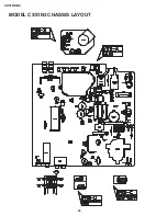
Page 20: ...20 CX51N3 N4 MODEL CX51N3 CHASSIS LAYOUT ...

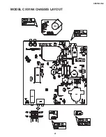
Page 21: ...21 CX51N3 N4 MODEL CX51N4 CHASSIS LAYOUT ...

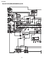
Page 22: ...22 CX51N3 N4 BLOCK DIAGRAM MAIN BLOCK ...

Page 23: ...23 CX51N3 N4 ...

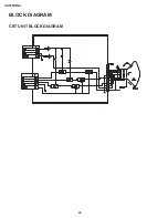
Page 24: ...24 CX51N3 N4 BLOCK DIAGRAM CRT UNIT BLOCK DIAGRAM L3 ...

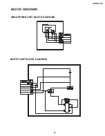
Page 25: ...25 CX51N3 N4 BLOCK DIAGRAM HEADPHONE UNIT BLOCK DIAGRAM BURST UNIT BLOCK DIAGRAM ...

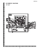
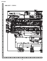
Page 26: ...27 CX51N3 N4 A B C D E F G H I J 1 2 3 4 5 6 7 8 9 10 CRT UNIT SCHEMATIC DIAGRAM ...

Page 27: ...28 CX51N3 N4 A B C D E F G H I J 1 2 3 4 5 6 7 8 9 10 MAIN UNIT CX51N3 ...

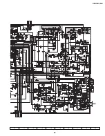
Page 28: ...29 CX51N3 N4 10 11 12 13 14 15 16 17 18 19 ...

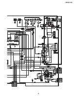
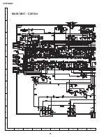
Page 29: ...30 CX51N3 N4 MAIN UNIT CX51N4 A B C D E F G H I J 1 2 3 4 5 6 7 8 9 10 ...

Page 30: ...31 CX51N3 N4 10 11 12 13 14 15 16 17 18 19 ...

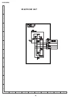
Page 31: ...32 CX51N3 N4 A B C D E F G H I J 1 2 3 4 5 6 7 8 9 10 HEADPHONE UNIT ...

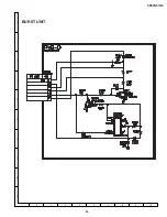
Page 32: ...33 CX51N3 N4 A B C D E F G H I J 1 2 3 4 5 6 7 8 9 10 BURST UNIT ...

Page 33: ...chigi 329 2193 Japan COPYRIGHT 2002 BY SHARP CORPORATION ALL RIGHTS RESERVED No part of this publication may be reproduced stored in a retrieval system or transmitted in any form or by any means electronic mechanical photocopying recording or otherwise without prior written permission of the publisher D SEM P SREC TQ1417 S OCT 2002 Printed in JAPAN MY KY ...

Reviews: