

16-1
16-2
CX51N3/N4
16
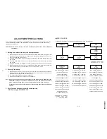
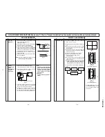
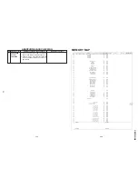
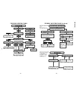
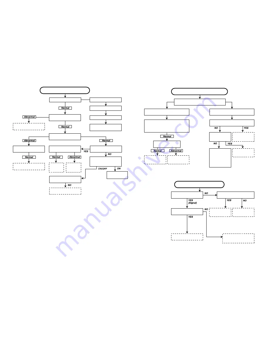
TROUBLE SHOOTING TABLE
NO RASTER
Blown out.
Replace the fuse.
Check IC701, D701 and
C705.
The fuse is again blown out.
Does horizontal circuit
oscillate ?
Check Q752 and IC801.
D1001 (Power LED Red
dimly) turns on or turns
ON/OFF.
Check T701 pin (11) voltage
(Approx. 310V at 220V AC)
Check F701.
Check Secondary Main+B
(Approx. 130V)
Check CRT connector
K1-K5 bias.
Check
C878.
Check
IC801.
Checking the
protector circuit.
Check R619 and R618.
D1001 (Power LED Red
brightly) turns on.
Check IC702, IC1080, D751
Check R701, R707
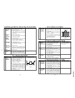
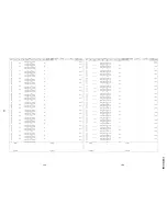
TROUBLE SHOOTING TABLE
(Continued)
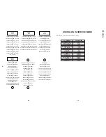
NO PICTURE, NO SOUND
Does noise signal appear at
pin (44) of IC801 ?
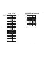
NO SOUND
No snow noise.
Does noise or signal appear at pin (40)
of IC801 ?
Noise increases but no signal is
received.
Check the tuner supply voltage LB must
be approx. 5V, BT must be approx. 32V.
and CH preset data check.
Check the tuner AGC at
TP201.
Does noise or
signal appear at
pin (38) of IC801 ?
Check IC801 and
its related circuit.
Check pin (1) of
SF201, Tuner and
related circuit.
Check pin (37) of
IC801 and related
circuit.
Check Q253, Q254
and related circuit.
Check IC801.
Check C356 and
peripheral circuit.
Check pin (27) of
IC801, Tuner and
related circuit.
Check pin(38) of
IC801.
Does the noise level increase at max.
Contrast, Brightness and Sound controls ?
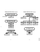
CIRCUITS TO BE CHECKED:
»
Tuner.
»
PIF.
»
Automatic Gain Control.
»
(5V), (32V) Power Source.
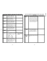
CIRCUITS TO BE CHECKED:
»
Sound system pins (28)
and (44) of IC801.
»
Sound Detector Circuit.
»
Sound Switch and Att.
Control.
»
Audio Output Circuit.
Does signal appear at pins
(2) and (4) of IC302 ?
Check P301, P302, IC301
and peripheral circuit.
Check Q321, pins(4) and (6)
of IC801 and peripheral
circuit.
Does signal appear at pins(28)
of IC801?
Summary of Contents for CX51N3
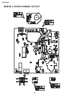
Page 20: ...20 CX51N3 N4 MODEL CX51N3 CHASSIS LAYOUT ...
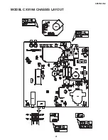
Page 21: ...21 CX51N3 N4 MODEL CX51N4 CHASSIS LAYOUT ...
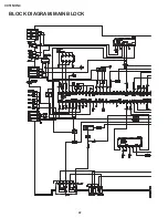
Page 22: ...22 CX51N3 N4 BLOCK DIAGRAM MAIN BLOCK ...
Page 23: ...23 CX51N3 N4 ...
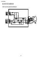
Page 24: ...24 CX51N3 N4 BLOCK DIAGRAM CRT UNIT BLOCK DIAGRAM L3 ...
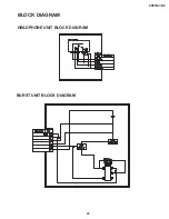
Page 25: ...25 CX51N3 N4 BLOCK DIAGRAM HEADPHONE UNIT BLOCK DIAGRAM BURST UNIT BLOCK DIAGRAM ...
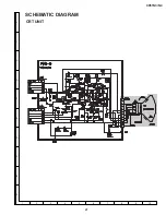
Page 26: ...27 CX51N3 N4 A B C D E F G H I J 1 2 3 4 5 6 7 8 9 10 CRT UNIT SCHEMATIC DIAGRAM ...
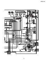
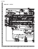
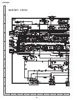
Page 27: ...28 CX51N3 N4 A B C D E F G H I J 1 2 3 4 5 6 7 8 9 10 MAIN UNIT CX51N3 ...
Page 28: ...29 CX51N3 N4 10 11 12 13 14 15 16 17 18 19 ...
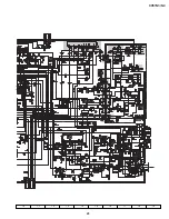
Page 29: ...30 CX51N3 N4 MAIN UNIT CX51N4 A B C D E F G H I J 1 2 3 4 5 6 7 8 9 10 ...
Page 30: ...31 CX51N3 N4 10 11 12 13 14 15 16 17 18 19 ...
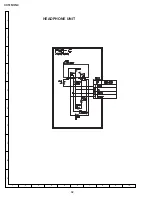
Page 31: ...32 CX51N3 N4 A B C D E F G H I J 1 2 3 4 5 6 7 8 9 10 HEADPHONE UNIT ...
Page 32: ...33 CX51N3 N4 A B C D E F G H I J 1 2 3 4 5 6 7 8 9 10 BURST UNIT ...


