


3
3-1
3-2
CX51N3/N4
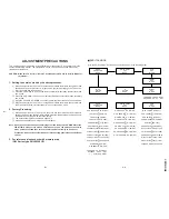
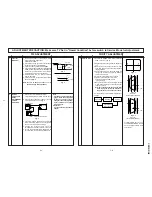
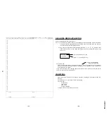
ADJUSTMENT PRECAUTIONS
This model’s setting are adjusted in two different ways: though the I
2
C bus control and in the
conventional analog manner. The adjustments via the I
2
C bus control include preset-only
items and variable data.
CAUTION: Make sure TV Set is in "Normal" Condition before switch to Service Mode for
adjustment.
1. Setting the service mode by the microprocessor.
1
Make a short-circuit 137 and 138 for a second and release to switch to the service mode
position and the microprocessor is in input mode. (Adjustment through the I
2
C bus con-
trol). (Use JWS Key to set as well).
2
Press the CH DOWN / UP key on the remote controller to get ready to select the mode
one by one.
3
Press the CH DOWN / UP key on the remote controller to select the modes reversibly
one by one.
4
Using the VOLUME UP/ DOWN key on the remote controller, the data can be modified.
5
Make a short-circuit 137 and 138 for a second and release to switch to the normal mode
(OFF) position and the microprocessor is in out of the service mode.
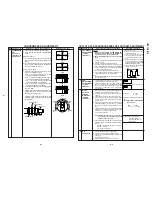
2. Factory Presetting.
1
Make a short-circuit JA137 and JA138, then turn ON the main power and release to
switch to service mode position. Initial values are automatically preset, only when a new
EEPROM is used (Judge with the first 4 bytes).
2
The initial data are preset as listed in pages 4-6.
3
Make sure the data need modify or not (Initial data).
Note: Once the chassis has been assembly together and ready to be POWER ON for the
FIRST TIME, make sure to make a short-circuit 137 and 138 switch to the service
mode position first and then turn on the main power switch. (See 2-1 above).
Precaution: If haven’t done this initiation, it may possibly generate excessive Beam
current.
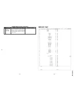
3. For reference please check with memory map
(GA1 Series type RH-iX3368CE)
Ë
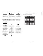
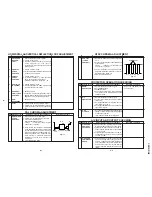
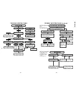
SERVICE MODE
(1) In the Service Mode, Key is used to select the mode in the following order.
AGC &
GEOMETRIC
MODE
↓
AGC TAKE OVER POINT (AGC)
↓
VERTICAL SLOPE (V-LIN)
↓
VERTICAL AMP (V-AMP)
↓
VERTICAL SHIFT (V-CENT)
↓
HORIZONTAL SHIFT (H-CENT)
↓
EAST-WEST WIDTH (H-SIZE)
↓
HORIZONTAL PARALLELOGRAM (EW//)
↓
EAST-WEST PARABOLA/WIDTH (PARA)
↓
EAST-WEST UPPER COR. PB (COR(U))
↓
EAST-WEST LOWER COR. PB (COR(L))
↓
EAST WEST TRAPEZIUM (TRAPE)
↓
HORIZONTAL BOW (HB)
↓
S-CORRECTION (S-COR)
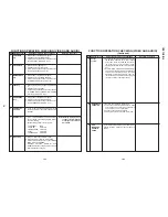
WHITE POINT
ADJ.
MODE
↓
W.P RED STD. W.T. (DRI-RS)
↓
W.P. GREEN STD. W.T.(DRI-GS)
↓
W.P.BLUE STD. W.T. (DRI-BS)
↓
W.P. RED COOL W.T.(DRI-RC)
↓
W.P. GREEN COOL W.T.(DRI-GC)
↓
W.P. BLUE COOL W.T.(DRI-BC)
↓
W.P. RED WARM W.T.(DRI-RW)
↓
W.P. GREEN WARM W.T.(DRI-GW)
↓
W.P. BLUE WARM W.T. (DRI-BW)
SUB
ADJ.
MODE
↓
MAX VOLUME (SUB-VOL)
↓
SUB CONTRAST (SUB-CON)
↓
SUB COLOUR (SUB-COL)
↓
SUB BRIGHTNESS (SUB-BRI)
↓
SUB TINT (SUB-TINT)
↓
SUB SHARPNESS (SUB-SHP)
↓
MAX HOTEL VOLUME (HTL-VOL)
↓
HOTEL PROGRAM NO(HTL-PRG)
↓
OSD RGB REFERENCE (RGB)
↓
BLACK LEVEL OFFSET R(CUT-R)
↓
BLACK LEVEL OFFSET G(CUT-G)
↓
CATHODE DRIVE LEVEL(CDL)
FORWARD : CH DOWN KEY
REVERSE : CH UP KEY
* ( ) means OSD display.
FORWARD : CH DOWN KEY
REVERSE : CH UP KEY
AGC &
GEOMETRIC
MODE
WHITE POINT
ADJ.
MODE
SUB
ADJ.
MODE
Y-DELAY
ADJ.
MODE
MISC.
OPTION
MODE
IC
OPTION
MODE
OFFSET
ADJ.
MODE
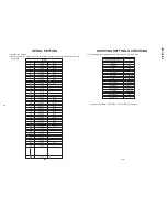
Summary of Contents for CX51N3
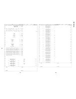
Page 20: ...20 CX51N3 N4 MODEL CX51N3 CHASSIS LAYOUT ...
Page 21: ...21 CX51N3 N4 MODEL CX51N4 CHASSIS LAYOUT ...
Page 22: ...22 CX51N3 N4 BLOCK DIAGRAM MAIN BLOCK ...
Page 23: ...23 CX51N3 N4 ...
Page 24: ...24 CX51N3 N4 BLOCK DIAGRAM CRT UNIT BLOCK DIAGRAM L3 ...
Page 25: ...25 CX51N3 N4 BLOCK DIAGRAM HEADPHONE UNIT BLOCK DIAGRAM BURST UNIT BLOCK DIAGRAM ...
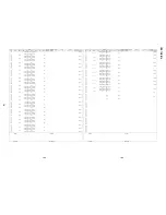
Page 26: ...27 CX51N3 N4 A B C D E F G H I J 1 2 3 4 5 6 7 8 9 10 CRT UNIT SCHEMATIC DIAGRAM ...
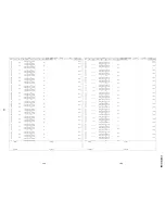
Page 27: ...28 CX51N3 N4 A B C D E F G H I J 1 2 3 4 5 6 7 8 9 10 MAIN UNIT CX51N3 ...
Page 28: ...29 CX51N3 N4 10 11 12 13 14 15 16 17 18 19 ...
Page 29: ...30 CX51N3 N4 MAIN UNIT CX51N4 A B C D E F G H I J 1 2 3 4 5 6 7 8 9 10 ...
Page 30: ...31 CX51N3 N4 10 11 12 13 14 15 16 17 18 19 ...
Page 31: ...32 CX51N3 N4 A B C D E F G H I J 1 2 3 4 5 6 7 8 9 10 HEADPHONE UNIT ...
Page 32: ...33 CX51N3 N4 A B C D E F G H I J 1 2 3 4 5 6 7 8 9 10 BURST UNIT ...


