background image

CD-BA120/125

– 36 –

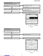
If the level is not normal, check around pins 27~29 on IC1.

1. Is focus servo activated? (Waveform drawing 36-2)

 Pins 1~11 on IC1
Check the laser diode driver Q3 peripheral circuit.
Focus error circuit (pins 20 and 21 on IC1)

When a disc is loaded, start playback operation.

2. Does DRF change from "L" to "H"?

Is the disc rotating?

3. Is the HF waveform normal?  (Waveform drawing 36-3)

Check the spin system.

If the disc is spinning and a HF waveform is generated,
DRF will go H.

Figure 36-1

Check the laser diode driver Q3 peripheral circuit.

(1) Focus-HF system check

Although a CD is inserted and the cover is closed, "NO
DISC" is displayed.

1. Did the pickup move to the PICKUP-IN Switch (SW4)

position?

Sled motor (M2)

Press the OPEN/CLOSE switch (SW1) without inserting a
disc, and try starting the playback operation.

2. Does the focus (lens) move up and down?
    (Waveform drawing 36-1).

Check the focus peripheral circuit.

3. Is the laser lit?

Spindle motor (M1).

4. Is the turntable rotating?

Figure 36-2

Figure 36-3

Yes

Yes

Yes

No

No

No

No

No

No

No

Yes

Yes

No

T

FDO

TDO

Stopped

CH1=500mV

DC   10:1

CH3=500mV

DC   10:1

500ms/div

(500ms/div)

NORM:20kS/s

1

3

=Record Length=

Smoothing :   ON

CH1  :      0.000V
CH2  :          0.0V

Main  :      100K
Zoom  :         2K

Mode  :   AUTO
Type   :   EDGE CH1
Delay  :                   0.0ns
Hold off  :                0.2us

CH3  :      0.000V
CH4  :        0.00V

BW   : FULL

=Trigger=

=Filter=

=Offset=

CH1
  v/DIV
  500mV

T

FDO

DRF

TE

Stopped

CH1=500mV

DC   10:1

CH2=10V

DC   10:1

CH3=1V

DC   10:1

500ms/div

(500ms/div)

NORM:20kS/s

1

2

3

=Record Length=

Smoothing :   ON

CH1  :      0.000V
CH2  :          0.0V

Main  :      100K
Zoom  :         2K

Mode  :   AUTO
Type   :   EDGE CH1
Delay  :                   0.0ns
Hold off  :                0.2us

CH3  :        0.00V
CH4  :        0.00V

BW   : FULL

=Trigger=

=Filter=

=Offset=

-3div

-1div

0div

+1div

+3div

CH  Position  To

CH2
  Position
  0.20div

Vp-p=1.0V~1.3V

0.5mV/div,0.5

µ

sec/div

Summary of Contents for CD-BA120

Page 1: ...SPLAY 45 REPLACEMENT PARTS LIST EXPLODED VIEW PACKING OF THE SET FOR U S A ONLY In the interests of user safety the set should be restored to its original condition and only parts identical to those specified be used SERVICE MANUAL This document has been published to be used for after sales service only The contents are subject to change without notice CD BA120 Mini Component System consisting of ...

Page 2: ...R TO THE OPERATION MANUAL IMPORTANT SERVICE NOTES FOR U S A ONLY BEFORE RETURNING THE AUDIO PRODUCT Fire Shock Hazard Before returning the audio product to the user perform the following safety checks 1 Inspect all lead dress to make certain that leads are not pinched or that hardware is not lodged between the chassis and other metal parts in the audio product 2 Inspect all protective devices such...

Page 3: ...Disc Skip Button 14 CD Track Down Review Button 3 TUNER Preset Down Button 3 TAPE 2 Rewind Button 15 CD Track Up Cue Button 3 TUNER Preset Up Button 3 TAPE 2 Fast Forward Button 16 CD Open Close Button 17 Timer Set Indicator 18 On Stand by Button 19 Timer Sleep Button 20 Clock Button 21 Function Selector Buttons 22 Equalizer Mode Selector Extra Bass Demo Mode Button 23 Volume Up Down Buttons 24 He...

Page 4: ...ion 12 Disc Number Select Buttons 13 Memory Button 14 Pause Button 15 Clear Button 16 Track Down Review Button 17 Track Up Cue Button 18 Disc Skip Button 19 Play Repeat Button 10 Stop Button 11 Random Button Tuner control section 12 Preset Up Down Buttons Tape control section 13 TAPE 1 Play Button 14 TAPE 2 Record Pause Button 15 TAPE 1 2 Stop Button 16 TAPE 2 Play Button 17 TAPE 2 Rewind Button 1...

Page 5: ...e clock starts operating from 0 second Seconds are not displayed And then the clock display will disappear after a few seconds To see the time display Press the CLOCK button The time display will appear for about 5 seconds Note The clock display will flash on and off at the push of the CLOCK button when the AC power supply is restored after a power failure occurs or after the AC power cord is disc...

Page 6: ... AC power cord x 1 Cable de alimentación de CA x 1 3 Listening to a CD Audición de discos CD 4 Listening to a tape Audición de una cinta 5 Listening to the radio Audición de la radio 6 Recording from CDs Grabaciones de discos CD 7 Sound control Control del sonido Label facing up Etiqueta hacia arriba To stop the playback Para detener la reproducción To stop the recording Para detener la grabación ...

Page 7: ... Be sure to remove the power supply plug from the wall outlet before starting to disassemble the unit 3 Take off nylon bands or wire holders where they need be removed when disassembling the unit After servicing the unit be sure to rearrange the leads where they were before disassembling 4 Take suffcient care on static electricity of integrated circuits and other circuits when servicing Figure 7 2...

Page 8: ... CD Player Unit H x2 1 2 J1 x3 J1 x3 K3 x2 K2 x2 K3 x2 CD Servo PWB CD Player Base K1 x1 ø3x8mm E1 x3 ø3x8mm D2 x2 D2 x2 D3 x1 Main PWB Headphones PWB D1 x7 ø3x10mm D1 x1 ø3x10mm F1 x9 ø3x10mm F2 x1 G1 x6 ø3x10mm Display PWB Open Cassette Holder Tape Mechanism CLAMP LEVER CAM GEAR RIB Figure 8 1 ...

Page 9: ...L1 x1 M1 x5 L1 x1 Loading Motor PWB CD Mechanism Cam Gear Driver Driver should be pried away from Speaker Box Direction of handle Speaker Box A2 x1 A1 x1 Speaker Box Speaker A3 x4 ø3 5x13mm STEP REMOVAL PROCEDURE FIGURE 1 Speaker 1 Net A1 x1 9 1 2 Duct Panel A2 x1 3 Screw A3 x4 9 2 ...

Page 10: ... roller C1 upwards Note When installing the pinch roller pay attention to the spring mounting position How to remove the belt TAPE 1 See Fig 10 4 1 Remove the main belt D1 x 1 pc from the motor side 2 Remove the FF REW belt D2 x 1 pc How to remove the belt TAPE 2 See Fig 10 4 1 Remove the main belt E1 x 1 pc from the motor side 2 Remove the FF REW belt E2 x 1 pc How to remove the motor See Fig 10 ...

Page 11: ...und the front end of connector so as to protect the optical pickup from electrostatic damage A1 x2 A1 x1 Loading Motor CD Base A1 x2 B1 x2 ø2 6 x6mm Shaft B2 x1 Stop Washer B3 x1 Gear B4 x1 CD Mechanism Pickup ADJUSTMENT MECHANISM SECTION Driving Force Check Torque Meter Specified Value Play TW 2111 Tape 1 Over 80 g Tape 2 Over 80 g Torque Check Torque Meter Tape 2 Play TW 2111 30 to 80 g cm 30 to...

Page 12: ...ot functioning 0203 Open Close SW High Low not functioning Error during skip operation 0302 Pickup in SW is not detected 0306 During Disc 1 search Open Close SW or Clamp SW or Disc SW do not change to low 0307 Clamp SW Low High not functioning 0308 Clamp SW High Low not functioning Since this CD system incorporates the following automatic adjustment functions readjustment is not needed when replac...

Page 13: ...eans micro micro farad and the unit of the capacitor without such a symbol is microfarad As to electrolyticcapacitor theexpression capacitance withstand voltage is used CH TH RH UJ Temperature compensation ML Mylar type P P Polypropylene type Schematic diagram and Wiring Side of P W Board for this model are subject to change for improvement without prior notice REF NO DESCRIPTION POSITION POSITION...

Page 14: ...RMAL Type EDGE CH2 Delay 2 924ms Hold off 0 2us CH3 0 00V CH4 0 00V BW FULL Trigger Filter Offset 1 IC2 24 6 IC2 25 T FDO PDO2 PDO1 Stopped CH1 500mV DC 10 1 CH3 1V DC 10 1 CH4 1V DC 10 1 500ms div 500ms div NORM 20kS s 1 4 3 Record Length Smoothing ON CH1 0 000V CH2 0 0V Main 100K Zoom 2K Mode AUTO Type EDGE CH2 Delay 0 0ns Hold off 0 2us CH3 0 00V CH4 0 00V BW FULL Trigger Filter Offset CH1 v DI...

Page 15: ...2 TIN1 FIN2 FIN1 IC3 M63001FP FOCUS TRACKING SPIN SLIDE DRIVER IC1 LA9235M SERVO AMP TO MAIN SECTION TO IC601 R CH L CH AGND DGND 5V B3 RCHO RVSS LVSS LCHO IC2 LC78641E SERVO SIGNAL CONTROL M SW1 OPEN CLOSE XL1 16 9344MHz 6 5 4 3 3 2 5 4 1 1 2 3 4 7 8 2 1 7 8 9 10 1 2 4 3 5 SW2 CLAMP SW3 DISC NUMBER M3 T T UP DOWN MOTOR 6 1 2 4 3 5 6 1 2 4 3 5 6 75 76 45 46 47 48 32 31 30 65 66 67 68 69 70 71 72 C...

Page 16: ...NF SWITCHING Q104 Q107 L T2 R T2 R T1 L T1 IC101 AN7345K PLAYBACK AND RECORD PLAYBACK AMP R L FM AM MPXIN STEREO AM RF IN AM OSC IN FM Q360 VT FM OSC OSC BUFF OSC X352 4 5MHZ AM BAND COVERAGE AM TRACKING T303 Q302 X351 456KHz MO ST VCO FM DET VCC GND AM IF CF351 AM IF IC303 LA1832S FM AM IF MPX AM MIX CF352 T351 FM RF FM OSC L312 CF303 T302 FM IF IC301 TA7358AP FM FRONT END BF301 CNP301 FM AM 22 3...

Page 17: ...907 D910 F902 1 6A 250V F901 3A 250V Vcc IC901 LA4282 POWER AMP BIAS T1 T2 AVDD KEY SW701 SW703 SW709 SW721 SW723 SW725 TO CD SECTION AC POWER SUPPLY CORD AC 120V 60Hz TF IC701 IX0336AW SYSTEM MICROCOMPUTER FL701 FL DISPLAY 11 10 5 2 7 1 3 33 32 78 91 80 100 27 31 13 11 10 6 5 4 1 2 99 92 33 31 45 46 7 11 1213 9 10 15 16 17 20 21 22 24 71 79 59 58 57 5554 53 52 51 4948 47 44 43 42 44 39 38 37 36 3...

Page 18: ...FO FO TR TR 1 2 3 4 5 6 7 8 8 3 6 7 1 4 5 2 PICKUP UNIT GND D PUIN SP SP SL SL 3 2 5 1 4 6 2 3 5 1 4 6 3 6 1 4 5 2 2 3 5 1 4 6 CD MOTOR PWB C 21 20 19 18 17 16 15 14 13 12 11 10 9 8 7 6 5 4 3 2 1 SLDO FDO TDO MUTE Vref STANDBY VCC1 SL SL GND TR TR FO FO FO FD TO B B B B B B M M R54 68K R53 68K R52 68K R51 68K CNP1 R56 68K R55 68K C6 100 10 C54 47 10 C55 0 01 C51 47 10 C53 0 001 R25 10K C7 10 16 C8...

Page 19: ...TROL A D SW D A B B 5 4 3 2 1 PCKIST VVDD VVSS PD02 PD01 73 80 79 78 77 76 75 74 FRAME SYNC DEFECT PROTECT EFM DECODE CLV CONTROL GENERAL SLICE LEVEL CONTROL PLL VCEC SLCO SLCIST HFL FR VDD5V CONT7 CONT6 VSS V vP FSEQ DEFECT EFMO RES DEF O C DISC_NO B 72 71 70 69 68 67 66 65 11 10 9 8 7 6 24 23 22 21 20 19 18 17 16 15 14 13 12 B 1 2 3 4 5 6 6 5 4 3 2 1 5 4 3 2 1 M 6 L CH B B 46 45 44 43 42 B 26 25...

Page 20: ...0K R602 330 R601 330 C603 22 25 R625 22K R615 3 9K C607 10 50 C609 0 1 C611 0 1 C623 1 50 C629 1 50 C617 1 50 C613 0 0027 C625 1 50 C627 1 50 R617 1K IC601 LC75341 AUDIO PROCESSOR C630 1 50 C610 0 1 C612 0 1 C618 1 50 C614 0 0027 C608 10 50 C606 22 50 C628 1 50 C626 1 50 C624 1 50 LUG1 MECHA BASE GND R102 10K R101 10K R103 4 7K Q101 KTA1266 GR C101 0 047 R157 100 Q102 KRC104 M C108 100 16 R104 1K ...

Page 21: ...O2 Hich CHROME 56K 56K A B C D E F G H I J K L M N O Q P T 18 1 CNP701 P27 12 C TO DISPLAY PWB MAIN PWB A1 1 3 C630 1 50 C605 0 022 C604 100 25 C610 0 1 C612 0 1 C618 1 50 R616 3 9K C614 0 0027 C608 10 50 C606 22 50 C628 1 50 C626 1 50 C624 1 50 R618 1K R131 1 5K C131 0 022 R135 10K C133 0 0033 C135 47 25 C129 22 25 C127 270 R133 100 C148 0 047 Q112 KTA1266 GR R148 22K R146 150 1 2W L103 100µH R14...

Page 22: ...1 ML C940 0 1 ML IC902 KIA7810AP VOLTAGE REGULATOR R926 10K C943 47 25 C944 0 022 ML C945 0 1 ML IC904 KIA7805AP VOLTAGE REGULATOR C933 68P Q90 KTA R930 220 R929 220 C954 100 35 R928 12K C955 47 50 C947 3300 25 D91 IN40 D911 IN4004S D913 IN4004S D914 IN400 D R C946 2200 35 ZD903 DZ6R2ASA R915 820 Q902 KRC102 M R914 22K 2 2 1 1 3 3 Q901 KRC102 M C918 220P R909 56K C914 470 25 R908 120 R906 1K R911 ...

Page 23: ... 12K C955 47 50 C947 3300 25 D917 IN4004S C956 47 50 ZD902 DZ300BSB R927 2 2K C957 47 50 C958 100 50 C959 100 50 D916 IN4004S D915 IN4004S C953 0 047 ML C952 0 047 ML D912 IN4004S D911 IN4004S D913 IN4004S D914 IN4004S CNP901 D910 RL204F D909 RL204F D907 RL204F D908 RL204F C950 0 047 ML F902 1 6A 250V F901 3A 250V C946 2200 35 C951 0 047 ML ZD903 DZ6R2ASA T801 POWER TRANSFORMER T F CNP801 SO801 AC...

Page 24: ... CH VD303 SVC211C R309 10K T301 T302 AM ANTENNA FM ANTENNA 2 C308 4 7P UJ D305 1SS133 R327 33 L312 R314 22 C314 0 0047 C316 0 022 C317 0 001 R313 33K C312 0 022 C315 0 0047 CF303 Q302 KTC3194Y OSC BUFF R316 4 7K R322 680 C318 100P R325 47K TP X352 4 5MHz C382 15P CH C381 12P CH R375 820 C384 0 001 R373 1K R372 1K R374 1K IC302 LC72131 PLL TUNER VSS AOUT AIN CL DI CE X IN X OUT 5 4 3 2 1 22 21 20 1...

Page 25: ... GND D GND P21 12 B TO MAIN SECTION T351 CF352 C370 1 50 R393 1K C358 1 50 R355 3 3K R388 3 9K C357 2 2 50 C356 0 001 C355 22P R352 1K C399 0 022 C398 100 10 C354 0 022 C353 0 022 C350 0 022 R353 270 CF351 10 16 12 11 10 9 8 7 6 5 4 3 2 1 IC303 LA1832S FM IF DET FM MPX AM IF VSM AM OSC OUT FM IF IN MO ST REG AM IF IN GND SD STEREO FM DET VCC IF OUT PHASE PHASE FM AM L CH OUT R CH OUT MPX IN MPX VC...

Page 26: ...73 72 71 70 69 68 67 66 65 64 63 62 61 60 59 58 57 56 55 54 53 52 51 54 53 52 31 32 33 51 1 2 3 4 5 6 7 8 9 10 11 12 13 14 15 16 17 18 19 20 21 22 23 24 25 26 27 28 29 30 50 49 48 47 46 45 44 43 42 41 40 39 38 37 36 35 34 33 32 31 81 82 83 84 85 86 87 88 89 90 91 92 93 94 95 96 97 98 99 100 100 6G 7G 8G 1G 2G 3G 4G 9G P14 P15 P16 2 1 13 12 11 10 9 8 7 2 1 3 4 5 6 B A M TAPE MECHANISM PWB E MM1 TAP...

Page 27: ... DI CD CLK RES OUT CLAMP SW D_GND 10 9 8 7 6 5 4 3 2 1 CNP12 P19 12 F TO CD SERVO PWB DISPLAY PWB A2 R726 2 2K R727 2 2K R728 2 2K R729 2 2K R719 1K R720 1K R721 1K R722 10K R724 1K IC701 IX0336AWZZ SYSTEM MICROCOMPUTER LED722 4204SRT R755 10K R725 1K R777 10K R776 10K R775 10K 3331 6 1273Y 8 SW710 OPEN CLOSE SW709 DISC SKIP RD09 100K RD08 56K RD01 680 SW701 POWER RD02 820 SW702 CLOCK SW703 TIMER ...

Page 28: ...4 15 15 17 16 18 CNP7 BR COLOR TABLE RD R OR YL GR BL VL GY WH W BK PK BROWN RED ORANGE YELLOW GREEN BLUE VIOLET GRAY WHITE BLACK PINK 1 29 FFC18 P30 6 G TO DISPLAY PWB CNP701 1 1 2 3 4 5 6 7 8 2 3 4 5 6 7 8 9 10 11 12 13 14 15 16 17 18 19 20 21 22 B C E E C B 1 1 2 3 2 3 3 2 1 1 2 3 1 2 3 4 5 6 7 8 9 10 1112 13 14 15 16 17 18 19 20 21 22 23 24 AM LOOP ANTENNA FM ANTENNA 1 2 3 L CH L CH R CH R CH ...

Page 29: ...117 C117 C123 C139 R143 C129 C135 Q111 C131 R139 R140 C138 Q110 C950 C951 D910 D909 D907 D908 R910 R911 R912 R913 C916 C917 C915 R909 C604 L104 Q903 C914 1 2 3 4 5 6 CNS901 P33 8 C TO POWER TRASFORMER 1 1 2 3 4 5 6 7 8 9 10 11 12 1 1 2 3 1 2 3 2 3 4 5 6 7 8 9 10 11 12 2 3 4 5 6 7 8 9 10 11 12 15 14 13 18 17 16 21 20 19 24 23 22 E C B E C B E C B E C B B C E 1 2 3 1 2 3 B C E 1 2 3 1 2 3 1 2 3 4 5 ...

Page 30: ...715 R XL701 30 31 35 40 45 50 51 55 60 65 70 85 90 95 81 80 75 1 5 10 15 20 25 100 C701 FL701 3 2 1 3 2 1 B B C E C E 3 5 7 9 11 13 15 17 18 16 1412 10 8 6 4 2 FROM MAIN PWB P28 5 H CNP701 18 CNP12 P32 5 A TO CD SERVO PWB RD WH GY WH GY WH GY WH GY WH BR COLOR TABLE RD R OR YL GR BL VL GY WH W BK PK BROWN RED ORANGE YELLOW GREEN BLUE VIOLET GRAY WHITE BLACK PINK 20 19 18 17 16 15 14 13 12 11 10 9 ...

Page 31: ...10 R711 R708 SW723 REC PAUSE SW716 TUNING TIME DOWN SW724 TUNING TIME UP SW713 VOLUME DOWN Q706 Q704 Q705 SW712 VOLUME UP SW711 X BASS DEMO 1 2 3 B C E B C E B C E 1 3 5 7 9 11 13 2 1 3 5 7 9 11 13 15 17 18 16 1412 10 8 6 4 2 4 6 8 10 12 FROM MAIN PWB P28 5 H CNP701 1 FFC18 FFC13 13 1 TO TAPE MECHANISM PWB P33 10 A 33 32 31 30 29 28 27 26 25 24 23 22 21 20 19 18 17 16 15 14 13 12 11 0 CNP701 CNP70...

Page 32: ... GY WH GY WH RD WH GR WH GR WH BL PK WH YL BK 1 2 3 4 5 6 7 8 1 2 3 4 5 6 7 8 1 2 3 4 5 6 7 3 4 1 2 5 6 7 PICKUP UNIT 306 CD SERVO PWB B CD MOTOR PWB C SW4 PICKUP IN M2 SLED MOTOR 1 2 3 4 5 6 1 2 3 4 5 6 1 2 3 4 5 6 CNP3A E C B B C E 1 2 3 IC2 IC3 R48 C46 R21 R40 R45 R22 R46 R95 R94 C30 R82 C40 R84 R81 C43 R83 C80 R12 C23 R79 R13 C21 C81 R11 C25 R14 C22 R10 C20 R8 C27 C42 C26 R15 C82 C29 R4 R3 R54...

Page 33: ... DISPLAY PWB BR COLOR TABLE RD R OR YL GR BL VL GY WH W BK PK BROWN RED ORANGE YELLOW GREEN BLUE VIOLET GRAY WHITE BLACK PINK 5 6 4 3 2 1 WH WH BR BR YL YL CNS901 PT801 POWER TRANSFORMER CNP901 P29 12 B TO MAIN PWB 1 2 3 CNS101B 2 3 1 WH BK PK CNS101A 2 3 1 WH BK PK CNP101 P29 12 G TO MAIN PWB CNP102 P29 10 H TO MAIN PWB CNS102A CNS102B BL GR WH PK WH BK 6 5 4 3 2 1 6 5 4 3 2 1 BL GR WH PK WH BK 6...

Page 34: ... 57V 3 2 1 PIN NO VOLTAGE Q903 4 9V 0V 4 9V 3 2 1 PIN NO VOLTAGE IC704 0V 3 0V 3 3V 3 3V 0V 0V 0V 1 6V 1 6V 1 6V 1 6V 1 6V 1 6V 1 6V 1 7V 4 7V 0V 1 6V 0V 2 4V 3 3V 0V 1 6V 3 0V 0V 3 3V 0V 0 7V 0V 0V 0V 0V 0V 1 6V 3 3V 0V 1 6V 1 6V 1 6V 1 6V 0V 2 1V 2 1V 0V 3 3V 3 5V 3 3V 3 3V 3 3V 1 6V 1 6V 1 5V 0V 1 5V 3 0V 3 3V 1 8V 3 0V 0V 0V 0V 1 7V 2 4V 0V 9 8 7 6 5 4 3 2 1 30 29 28 27 26 25 24 23 22 21 20 19...

Page 35: ... CD disc tray with the brush side down then press the play button You will hear music for about 20 seconds and the CD player will automatically stop If it continuous to tum press the stop button 1 2 3 The CD lens cleaner should be effective for 30 50 operations however if the brushes become worn out earlier then please the cleaner disc If the CD cleaner brushes become very wet then wipe off any ex...

Page 36: ...without inserting a disc and try starting the playback operation 2 Does the focus lens move up and down Waveform drawing 36 1 Check the focus peripheral circuit 3 Is the laser lit Spindle motor M1 4 Is the turntable rotating Figure 36 2 Figure 36 3 Yes Yes Yes No No No No No No No Yes Yes No T FDO TDO Stopped CH1 500mV DC 10 1 CH3 500mV DC 10 1 500ms div 500ms div NORM 20kS s 1 3 Record Length Smo...

Page 37: ... and then try starting the play operation 3 Spin system check The spin driver circuit is OK 1 The turntable rotates a little Waveform drawing 37 2 Check around pin 25 on IC2 pins 15 and 16 on IC3 and CNS3A B 2 The turntable doesn t rotate T T TE DRF Stopped CH1 10V DC 10 1 CH2 1V DC 10 1 100ms div 100ms div NORM 100kS s 2 1 Record Length Smoothing ON CH1 0 0V CH2 0 00V Main 100K Zoom 2K Mode NORMA...

Page 38: ...orm is normal but the TOC data cannot be read Check the PDO waveform Figure 38 1 Check around pins 1 6 on IC2 Figure 38 1 Figure 38 2 T FDO PDO2 PDO1 Stopped CH1 500mV DC 10 1 CH3 1V DC 10 1 CH4 1V DC 10 1 500ms div 500ms div NORM 20kS s 1 4 3 Record Length Smoothing ON CH1 0 000V CH2 0 0V Main 100K Zoom 2K Mode AUTO Type EDGE CH2 Delay 0 0ns Hold off 0 2us CH3 0 00V CH4 0 00V BW FULL Trigger Filt...

Page 39: ... 21 FE 22 RFEV 28 RF 1 PDO1 2 PDO2 3 VVSS 4 PCKIST 5 VVDD 6 FR 7 HFL 8 SLCIST 9 SLCO 10 EFMIN 11 JITTV 12 JITTC 13 BH 14 PH RFENV 15 FE 16 TE 25 SPDO 26 SLDO 27 FG 28 LASER 29 CONT1 30 CONT2 CONT3 CONT4 CONT5 31 32 33 34 PCK 35 C2F 36 VDD 37 DOUT 38 FSX 39 EFLG 40 TEST EFMO DEFECT FSEQ V P CONT7 CONT6 VSS VDD DRF RES WRQ INT DO DI CL CE 17 VREF 18 ADAVDD 19 ADAVSS 20 PHREF 21 BHREF 22 TBLO 23 TDO ...

Page 40: ...5 SPDO Output 1 2VDD Output terminal for spindle control D A output 26 SLDO Output 1 2VDD Output terminal for sled control D A output 27 FG Input FG signal input terminal When not used connect to 0V 28 LASER Output L LASER ON OFF control terminal 29 CONT1 In Output Input mode General purpose input output terminal 1 Controlled with serial data command 30 CONT2 In Output Input mode General purpose i...

Page 41: ...al 67 DI Input interface Data input terminal 68 DO Output L Data output terminal 69 INT Output H Interruption signal output terminal 70 WRQ Output H Interruption signal output terminal 71 RES Input Reset input terminal of LC78640 When turning on power set it at L 72 DRF Output L Focus ON detection terminal 73 VDD5V Power terminal for microcomputer interface 74 VSS Ground terminal of digital system...

Page 42: ...TPUT 23 P21 DT Output DATA OUTPUT 24 P20 DO Output DATA INPUT 25 AVss AVSS ANALOG GROUND 26 ANI7 TUN SM Input TUNER SIGNAL METER INPUT P17 M BUSY Input COMMUNJCATE TO MPEGU COM M_BUSY 27 ANI6 NO USE Input GND 28 ANI5 SPEANA 2 Input SPEANA DATA INPUT 16 KHz 29 ANI4 SPEANA 1 Input SPEANA DATA INPUT 1 KHz 30 ANI3 SPEANA 0 Input SPEANA DATA INPUT 63 KHz 31 33 ANI2 ANI0 KEY2 KEY0 Input KEY INPUT 34 AVD...

Page 43: ...H1 output offset control 4 OUT1 CH1 inverted output 5 OUT1 CH1 non inverted output 6 OUT2 CH2 inverted output 7 OUT2 CH2 non inverted output 8 14 GND GND 15 OUT3 CH3 non inverted output 16 OUT3 CH3 inverted output 17 IN3 CH3 inverted input 18 VCC1 Power supply 1 CH1 CH2 CH3 19 STANDBY STANDBY signal input 20 VRFE CH1 CH4 Reference voltage input 21 MUTE Mute signal input CH6 22 IN5 CH5 inverted inp...

Page 44: ...ef CONTROL CIRCUIT CONTROL CIRCUIT CONTROL CIRCUIT LOUT LBASS 0 1uF LIN LSEL0 L4 L3 L2 L1 R1 R2 R3 R4 RSEL0 R1N RTRE LTRE RBASS 0 1uF ROUT Yref VDD CL DI CE YSS CCB INTERFACE CD Tuner Tape Video 24 23 22 21 20 19 18 17 16 15 14 13 1 2 3 4 5 6 7 8 9 10 11 12 LC75341 DI CE VSS LOUT LBASS LTRE LIN LSEL0 L4 L3 L2 L1 CL VDD VREF ROUT RBASS RTRB RIN RSEL0 R4 R3 R2 R1 ...

Page 45: ...p e n r c s 2G U T V W a b k j h f m d g p e n r c s 3G U T V W a b k j h f m d g p e n r c s 4G U T V W a b k j h f m d g p e n r c s 5G U T V W a b k j h f m d g p e n r c s 6G U T V W a b k j h f m d g p e n r c s 7G U T V W a b k j h f m d g p e n r c s 8G U T V W a b k j h f m d g p e n r c s 9G 2G 3G 4G 5G 6G 7G 8G 9G 1G a b c d f g m e r p n h j k V T U W s L R ...

Page 46: ... M E M O 46 CD BA120 125 ...

Page 47: ...e without lead wire VC TQ Square type without lead wire VC CY Square type without lead wire VC CZ Square type without lead wire VC J The 13th character represents capacity difference J 5 K 10 M 20 N 30 C 0 25 pF D 0 5 pF Z 80 20 If there are no indications for the electrolytic capacitors error is 20 Resistors VRD Carbon film type VRS Carbon film type VRN Metal film type VR MF Cylindrical type with...

Page 48: ...AM OSC T351 RCILI0019AWZZ J AD AM IF COILS L61 VP XHR82K0000 J AC 0 82 µH L62 VP XH2R2K0000 J AB 2 2 µH Choke L103 VP DH101K0000 J AB 100 µH Choke L104 VP MK331K0000 J AB 330 µH Choke L312 RCILR0056AWZZ J AB FM RF L351 352 VP DH101K0000 J AB 100 µH Choke L701 VP DH101K0000 J AB 100 µH Choke VIBRATORS X351 92LCRSTL1425A J AF Crystal 456 kHz X352 RCRSP0002AWZZ J AH Crystal 4 5 MHz XL1 92LCRSTL1746AT...

Page 49: ...J AA 15 pF 50V C704 VCCSMN1HL180J J AA 18 pF 50V C705 VCEAZA1AW107M J AB 100 µF 10V Electrolytic C707 708 RC EDZ105AF1H J AB 1 µF 50V Electrolytic C710 VCEAZA1EW476M J AB 47 µF 25V Electrolytic C711 712 RC EZD106AF1C J AC 10 µF 16V Electrolytic C713 VCEAZA1HW104M J AB 0 1 µF 50V Electrolytic C714 VCTYMN1CY103N J AA 0 01 µF 16V C715 VCEAZA1HW335M J AB 3 3 µF 50V Electrolytic C716 VCTYBT1EF223Z J AA...

Page 50: ...3 3 kohms 1 8W R625 VRD ST2CD223J J AA 22 kohms 1 6W R702 704 VRD MN2BD102J J AA 1 kohm 1 8W R705 717 VRD ST2CD102J J AA 1 kohm 1 6W R719 721 VRD MN2BD102J J AA 1 kohm 1 8W R722 VRD MN2BD103J J AA 10 kohm 1 8W R724 VRD ST2CD102J J AA 1 kohm 1 6W R725 VRD MN2BD102J J AA 1 kohm 1 8W R726 729 VRD ST2CD222J J AA 2 2 kohms 1 6W R732 VRD ST2CD102J J AA 1 kohm 1 6W R733 737 VRD MN2BD102J J AA 1 kohm 1 8W...

Page 51: ...ment Item 201 2 GDORF0076AWSA J AE Holder Cassette Tape 1 201 3 GDORF0077AWSA J AE Holder Cassette Tape 2 201 4 GCOVA1270AWSA J AH Cover Cassette Tape 1 201 5 GCOVA1271AWSA J AH Cover Cassette Tape 2 201 6 HDECQ0541AWSA J AE Panel Cassette Tape 1 201 7 HDECQ0542AWSA J AE Panel Cassette Tape 2 201 8 HDECQ0543AWSA J AH Panel Amp 120 201 8 HDECQ0567AWSA J Panel Amp 125 201 10 JKNBZ0677AWSA J AG Knob ...

Page 52: ...n Manual 120 for Canada TINSK0103AWZZ J Operation Manual 125 for Canada TINSZ0532AWZZ J Operation Manual 120 for Central America Mexico TINSZ0533AWZZ J AB Quick Guide 120 for U S A Only TINSZ0534AWZZ J Operation Manual 125 for Central America Mexico TINSZ0538AWZZ J Quick Guide 125 for U S A Only TLABR1090AWZZ J AB Label Bar Code 120 TLABR1130AWZZ J Label Bar Code 125 TLABZ0711AWZZ J Label Feature ...

Page 53: ...CD BA120 125 6 A B C D E F G H 1 2 3 4 5 6 Figure 6 CD MECHANISM EXPLODED VIEW CD BA120 125 306 1 701 304 701 302 301 702 303 M1 703x4 305x2 SW4 M2 305 PWB C 306 2 306 3 306 704 ...

Page 54: ...2 201 16 201 3 201 23 PT801 201 22 201 8 PWB A3 611x3 610 225 225 268 620 201 21 201 21 201 201 20 201 26 201 27 201 1 616 201 24 620 MM1 MAIN BELT FLYWHEEL ASS Y TAPE1 FLYWHEEL ASS Y TAPE2 PWB A1 231x4 617x9 FL701 270 214 213 237x4 612 605x9 606x2 614 x7 610x3 610x2 610x2 271x2 226 201 25 201 10 201 15 201 13 201 14 201 12 201 11 221 219 208 612 222 606x2 220 209 230 Silicon grease FF REW ROLLER ...

Page 55: ... G H 1 2 3 4 5 6 CD BA120 125 248 CD MECHANISM 205 257 235 236 243 224 259 239 239 260 204 2 204 1 204 3 258 269 204 240 239x3 604x2 604x2 250x4 256 247 262 238 241 244 618 251 252 255 249 253 PWB B 239 254 246 232 263 234 M3 M3 PWB E 242 SW3 SW2 SW1 619 264 245 ...

Page 56: ...CD BA120 125 9 A B C D E F G H 1 2 3 4 5 6 Figure 9 SPEAKER EXPLODED VIEW 1 2 CP BA120 125 907 905x4 904 906 902 903 901 BK RD SPEAKER SP1 L CH SP2 R CH SPEAKER SP1 L CH SP2 R CH SP1 L CH SP2 R CH ...

Page 57: ...A120 125 A B C D E F G H 1 2 3 4 5 6 10 903 902 904x6 905 SP3 L CH SP4 R CH 901 WOOFER SP3 L CH SP4 R CH BLACK WHITE WOOFER SP3 L CH SP4 R CH GBOXS0042AWM1 CD BA125 ONLY Figure 10 SPEAKER EXPLODED VIEW 2 2 ...

Page 58: ...e Operation Manual SPAKC0895AWZZ BA120 SPAKC0897AWZZ BA125 Packing Case TLABR1090AWZZ BA120 TLABR1130AWZZ BA125 Label Bar Code FRONT SIDE OF SPEAKERS SPAKA0242AWZZ Packing Add Left Right TLABZ0712AWZZ Label Feature Tape2 TLABZ0711AWZZ BA120 TLABZ0718AWZZ BA125 Label Feature Tape1 92LN1885B Packing Add Bottom 92LN1885T Packing Add Top 92LV4974A Polyethylene Bag Bottom TOP FRONT A B A FRONT SPEAKER ...

Page 59: ...CD BA120 125 12 MEMO ...

Page 60: ...rieval system or transmitted in any from or by any means electronic mechanical photocopying recording or otherwise without prior written permission of the publisher A0002 2627NS HA I SC SL LAG SHARP CORPORATION Communication Systems Group Quality Reliability Control Center Higashihiroshima Hiroshima 739 0192 Japan Printed in Japan ...

Reviews: