5. Communication buffer and reset circuit
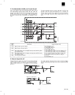
In the communication buffer circuit, the transmission signal (F-TXD)
and communication permit signal (F-DTR) from the copier are
received by the buffer IC 74HC14 (IC101), while the reception signal
(F-RXD) and communication request signal (F-DSR) transmitted from
the finisher to the copier are outputted from the transistor Q101 and
Q102.
The reset signal from the copier is also received by the IC101 and
inputted to the CPU’s reset terminal (active at L). In addition, the
reversion signal is inputted to the expansion I/O reset terminal (active
at H). For each signal, a protective diode is inserted between
+
5V and
GND.
Signal
name
Description
Logic (connector level)
F-TXD
Signal line from copier to finisher
Start bit detection at H
Usual (marking state) at L
F-RXD
Signal line from finisher to copier
Start bit detection at L
Usual (marking state) at L
F-DTR
Status display signal line for the signal showing communication permit
from finisher to copier
Communication from finisher to copier is inhibited at H
Communication from finisher to copier is permitted at L
F-DSR
Status display signal line for the signal showing communication request
from finisher to copier
No communication request from finisher to copier at H
Communication request from finisher to copier at L
F-RES
Hard rest signal from copier
Reset at H
Reset is released at L
74HC14
74HC14
74HC14
74HC14
IC101
IC101
IC101
IC101
+5V
+5V
+5V
R125
1
2
R113
4.7K
6
5
10
11
IC101
8
9
+5V
0.1U
RES/
RES
14
F-TXD
F-RXD
12
17
F-DTR
F-DSR
16
63
33
F-TXD
F-RXD
F-DTR
F-DSR
F-RES
C131
0.1U
from Copier
Q102
Q101
74HC14
R115
1K
4.7K
10K
10K
10K
10K
C118 0.1U
C117 1000p
C120 1000p
RT1N141C
RT1N141C
R126 4.7K
R114
4.7K
RXD0/P92
TXD0/P90
CPU
(IC03)
I/O
(IC11)
P95
P94
RES
RESET
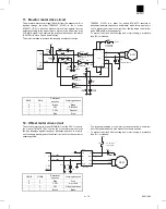
6. Sensor input circuit
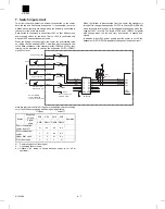
The signal from each sensor connected to 10 kohm pull-up resistance
and noise-removing 1000 pF capacitor, and connected through 10
kohm protective resistance to CPU, and expansion I/O Schmitt trigger
input port.
The sensor signal for transport system is input to the schmitt trigger
input port because the sensor input circuit is not provided with rectifier
circuit.
H.P.sensor
+5V
+5V
10K
1000PF
P**
10K
(IC02)
AMP
*1
*1:Rated Voltage Sircuit
CPU
Transport system sensor
240
+5V
+5V
10K
1000PF
PA or PB
10K
(IC03)
2
*2 Schumit trigger input port
I/O
AR-FN3
9 – 6
8/19/1999
Summary of Contents for AR-FN3
Page 20: ...15 15 15 15 16 AR FN3 8 19 1999 5 7 ...
Page 27: ... Rollers Paper guides AR FN3 7 2 8 19 1999 ...
Page 28: ...AR FN3 8 19 1999 7 3 ...
Page 29: ... Gears Others Sensors Belts AR FN3 7 4 8 19 1999 ...
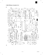
Page 51: ...3 Main PWB page arrangement 1 2 AR FN3 10 9 8 6 1999 ...
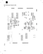
Page 52: ...Main PWB page arrangement 2 2 AR FN3 8 6 1999 10 10 ...

