LC-42SB45U
46
The LD1117 is a LOW DROP Voltage Regulator able to provide up to 800mA of Output Current, available even in adjustable version (Vref=1.25V).
Concerning fixed versions, are offered the following Output Voltages: 1.2V,1.8V,2.5V,2.85V, 3.0V 3.3V and 5.0V. The 2.85V type is ideal for
SCSI-2 lines active termination. The device is supplied in: SOT-223, DPAK, SO-8 and TO-220. The SOT-223 and DPAK surface mount packages optimize
the thermal characteristics even offering a relevant space saving effect. High efficiency is assured by NPN pass transistor. In fact in this case, unlike than
PNP one, the Quiescent Current flows mostly into the load. Only a very common 10µF minimum capacitor is needed for stability. On chip trimming allows
the regulator to reach a very tight output voltage tolerance, within ± 1% at 25°C. The ADJUSTABLE LD1117 is pin to pin compatible with the other
standard. Adjustable voltage regulators maintaining the better performances in terms of Drop and Tolerance.
Features
·
Low dropout voltage (1V TYP.)
·
2.85V Device performances are suitable for SCSI-2 active termination
·
Output current up to 800 mA
·
Fixed output voltage of: 1.2V, 1.8V, 2.5V, 2.85V, 3.0V, 3.3V, 5.0V
·
Adjustable version availability (Vrel=1.25V)
·
Internal current and thermal limit
·
Available in ± 1% (at 25°C) and 2% in full temperature range
·
Supply voltage rejection: 75dB (typ.)
2
.8. U721 (LD39080PT)
General Description
The LD39080 is a fast ultra low drop linear regulator which operates from 2.5V to 6V input supply. A wide range of output options are available. The
low drop voltage, low noise, and ultra low quiescent current make it suitable for low voltage microprocessor and memory applications. The device is
developed on a BiCMOS process which allows low quiescent current operation independently of output load current.
Features
·
0.8A Guaranteed output current
·
Ultra low dropout voltage (150mV typ. @ 0.8A load, 20mV typ. @150mA load)
·
Very low quiescent current (1mA typ. @ 0.8A load, 1µA max @ 25°C in off mode)
·
Logic-controlled electronic shutdown
·
Current and thermal internal limit
·
±
1.5% Output voltage tolerance @ 25°C
·
Fixed and ADJ output voltages: 1.22V, 1.8V, 2.5V, 3.3V, ADJ.
·
Temperature range: -40 to 125°C
·
Fast dynamic response to line and load changes
·
Stable with ceramic capacitor
·
Available in PPAK, DPAK and DFN8 (4x4mm)
2
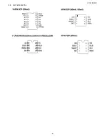
.9. U701/U708/U700/U550(M24C02-WDW6P TSSOP8)
DESCRIPTION
These I²C-compatible electrically erasable programmable memory (EEPROM) devices are organized as 2048/1024/512/256/128 x 8 (M24C16, M24C08,
M24C04, M24C02 and M24C01).
In order to meet environmental requirements, ST offers these devices in ECOPACK® packages. ECOPACK® packages are Lead-free and RoHS
compliant.
ECOPACK is an ST trademark. ECOPACK specifications are available at: www.st.com.
I²C uses a two-wire serial interface, comprising a bidirectional data line and a clock line. The devices carry a built-in 4-bit Device Type Identifier code (1010)
in accordance with the I²C bus definition.
The device behaves as a slave in the I²C protocol, with all memory operations synchronized by the serial clock. Read and Write operations are initiated by
a Start condition, generated by the bus master. The Start condition is followed by a device select code and Read/Write bit (RW), terminated by an
acknowledge bit.
When writing data to the memory, the device inserts an acknowledge bit during the 9th bit time, following the bus master’s 8-bit transmission. When data is
read by the bus master, the bus master acknowledges the receipt of the data byte in the same way. Data transfers are terminated by a Stop condition after
an Ack for Write, and after a NoAck for Read
.
.
FEATURES
·
Two-wire I²C serial interface
Summary of Contents for AQUOS LC-42SB45U
Page 6: ...LC 42SB45U 6 TV Front view TV Rear view ...
Page 11: ...2008 03 14 LC 42SB45U 11 3 DIMENSIONS ...
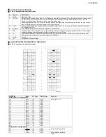
Page 50: ...LC 42SB45U 50 3 2 U102 LP2996MRX PSOP 8 3 2 1 Pin Connections and short description ...
Page 54: ...LC 42SB45U 54 3 8 U402 MX25L3205DMI 12G SOP 16 3 8 1 Block Diagram ...
Page 55: ...2008 03 14 LC 42SB45U 55 3 8 2 PIN CONFIGURATION ...
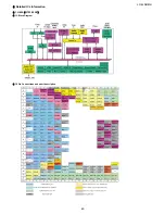
Page 56: ...LC 42SB45U 56 CHAPTER 6 BLOCK DIAGRAM WIRING DIAGRAM 1 MT5382 POWER MAGAGEMENT BLOCK DIAGRAM ...
Page 57: ...2008 03 14 LC 42SB45U 57 2 MAIN BOARD BLOCK DIAGRAM ...
Page 58: ...LC 42SB45U 58 3 WIRING DIAGRAM ...
Page 60: ...60 LC 42SB45U MAIN Unit Side B ...
Page 61: ...LC 42SB45U 1 POWER UNIT PRINTED WIRING BOARD POWER Unit Side A 61 ...
Page 62: ...LC 42SB45U POWER Unit Side B 62 ...
Page 64: ...64 LC 42SB45U IR Unit Side A 3 IR UNIT PRINTED WIRING BOARD IR Unit Side A Cn001 A2 ...


