background image

AM-900U

1 – 7

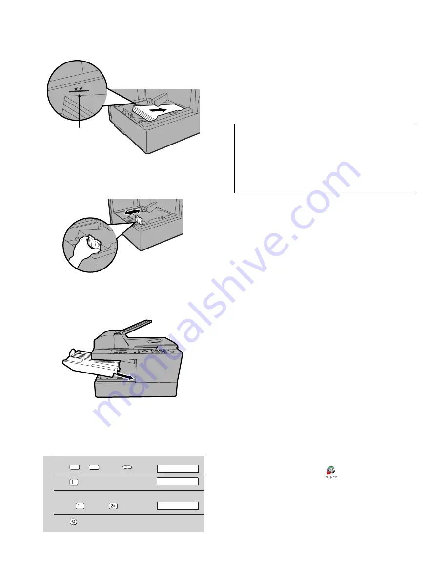
2) Insert a stack of paper into the tray, print side up.


Important!

 The stack of paper must not be higher than the paper

height line on the paper tray.

3) Squeeze the sides of the paper guide as shown and slide it to the

slot for the length of the paper you are loading.

4) Replace the output tray.

 If you loaded legal size paper (or you changed the paper size),

change the paper size setting as explained below.

7. Setting the paper size

The machine has been set at the factory to use letter size paper. If you
loaded legal size paper, you must change the paper size setting to
LEGAL.

8. Installing the software

To use the machine as a printer and scanner for your computer, you
must install the software and connect a USB cable. The CD-ROM that
comes with the machine contains the following software:

MFP Drivers:

 These consist of the printer driver that allows the

machine to be used as a printer, and the scanner driver that allows
you scan using TWAIN and WIA compliant applications.

Sharpdesk:

 This is an integrated software environment that makes

it easy to manage image files and launch applications. (Note that
Internet Explorer 5.5 or higher is required to install Sharpdesk; if
this is not installed, you will be prompted during the installation pro-
cedure to install Internet Explorer 6.0SP1

®

 from the CD-ROM.)

Minimum system requirements

Operating system:        Windows 98 SE

®

 / Me

®

 / 2000

®

 / XP

®

Port:                              USB 2.0 or 1.1 port

Display:                        800 x 600 (SVGA) with 256 colors or more

Free hard-disk space:  150 MB or more

Other requirements:     An environment in which the operating
                                     system can freely operate.

Comments:

• USB 2.0 Hi-Speed is only possible if your computer has a USB 2.0

port and you are using a USB 2.0 cable. In addition, the Microsoft
USB 2.0 driver must be preinstalled in your computer, or the USB
2.0 driver for Windows 2000/XP

®

 provided through Windows

Update must be installed. Note that USB 2.0 Hi-Speed is not possi-
ble in Windows 98 SE

®

 or Me

®

.

• To scan a legal size document (the maximum size) at 1200 dpi in

full color, at least 600 MB or more of free hard disk space is
required on the drive where your operating system is installed.

Installing the software

• A USB cable is required to connect the machine to your computer.

Please purchase a USB 2.0 or USB 1.0/1.1 cable. (If you wish to
use USB 2.0 Hi-Speed mode and your system meets the require-
ments for Hi-Speed mode, purchase a USB 2.0 cable.) The USB
cable will be connected during the software installation procedure.

• To install the software on Windows 2000/XP

®

 using the installer,

you must log in with administrator’s rights.

• The windows shown in the following procedure appear in Windows

XP

®

. The windows that appear in other versions of Windows may

be slightly different.

1) Make sure that the USB cable is not connected to your computer.

(The cable will be connected in Step 10.)

 If the USB cable is connected, a Plug and Play window will

appear. Click the Cancel button to close the window and discon-
nect the cable.

2) Insert the Sharp CD-ROM into your computer’s CD-ROM drive.

3) In Windows XP

®

, click the 

start

 button, click 

My Computer

, and

then double-click the CD-ROM icon.

In Windows 98/Me/2000

®

, double-click 

My Computer

 on the desk-

top and then double-click the CD-ROM icon.

4) Double-click the 

setup

 icon ( 

 ) in the CD-ROM window.

5) Follow the instructions in the windows that appear.

 When the 

Setup Type Selection

 window appears, select 

Stan-

dard

 to install all of the software components (this should normally

be selected). If you only wish to install certain components, select

Custom

 and then select the components that you wish to install.

Note:

 If you wish to select the folder where Sharpdesk is installed,

select 

Custom

.

Paper height line

1

Press

(or

) and then

.

2

Press

.

3

Select the paper size:
LETTER:

LEGAL:

4

Press

repeatedly to exit.

COPY

SCAN

MENU

The display briefly shows

your selection, then:

1:LETTER

Display:

COMMON SETTING

2: AUTO CLEAR

Summary of Contents for AM 900 - Digital Office Laser Copier

Page 1: ...PTION 1 Mechanical description 3 1 2 Disassembly and assembly procedures 3 18 CHAPTER 4 DIADRAMS 1 Block diagram 4 1 2 Wiring diagram 4 2 3 Point to point diagram 4 3 CHAPTER 5 CIRCUIT DESCRIPTION 1 Circuit description 5 1 2 Circuit description of control PWB 5 1 3 Circuit description of LIU PWB 5 19 4 Circuit description of power supply PWB 5 21 5 Circuit description of CIS unit 5 22 6 Circuit de...

Page 2: ...50 000 prints Service Engineer Fuser Fusing unit Refer to the P G No 5 901 DUNTK273DXH01 50 000 prints Service Engineer Paper transport Feed roller Refer to the P G No 3 29 NROLR2333XHZZ Cleaning as needed Unit AM 900 5 years or 50 000 prints of early either 1 Employing lead free solder This model employs lead free solder This is indicated by the LF symbol printed on the PWB and in the service man...

Page 3: ...inch 8 dots mm Vertical Standard 98 lines inch 3 85 lines mm Fine Halftone 196 lines inch 7 7 lines mm Super fine 391 lines inch 15 4 lines mm 256 levels FAX ONLY EXT TEL Based on Sharp Standard Chart at standard resolution excluding time for protocol signals i e ITU T phase C time only Scanner type Resolution Scan speed Compatibility Grayscale Color CIS Contact Image Sensor 300 600 x 300 dpi 300 ...

Page 4: ... HELP FAX key and SCAN key Press the FAX key and SCAN key simultaneously to print the HELP list a brief guide to the operation of the machine 13 FAX key Press this key to select fax mode When in fax mode press this key to select the Line Monitor function 14 Alarm indicator This blinks when the toner cartridge nears empty or the drum cartridge is near or at the end of its life This lights steadily ...

Page 5: ...rtion into the feeder to prevent possible double feeds 5 Automatic Document Feeder Capacity Number of pages that can be placed into the feeder at anytime is as follows Normal size max ADF 20 pages Special size single sheet only manual feed NOTE When you need to send or copy more pages than the feeder limit place additional pages in feeder when last page in feeder is being scanned Place additional ...

Page 6: ... into a jack which is not jack may result in damage to the machine or your telephone system If you do not know what kind of jack you have or need to have one installed contact the telephone company 2 Attaching the trays 1 Attach the document feeder tray Slide the output tray into the machine as shown When it stops lift the end slightly and push in so that the tray locks in place Important The outp...

Page 7: ... cartridge is guaranteed for 24 months after the date of manu facture indicated on the package 1 Press the side cover release open the side cover and then open the front cover Caution The fusing unit inside the print compartment becomes very hot during operation Do not touch the inside of the print com partment after the machine has been in operation 2 Remove the new drum cartridge from its packag...

Page 8: ...ach time you install a new drum cartridge follow the steps below to reset the drum counter to zero 5 Manually resetting the toner counter When a new toner cartridge is installed the toner counter is reset in Step 7 on the previous page The procedure below is normally not nec essary however it can be used in the event that you need to reset the toner manually 6 Loading printer paper You can load up...

Page 9: ...dows Update must be installed Note that USB 2 0 Hi Speed is not possi ble in Windows 98 SE or Me To scan a legal size document the maximum size at 1200 dpi in full color at least 600 MB or more of free hard disk space is required on the drive where your operating system is installed Installing the software A USB cable is required to connect the machine to your computer Please purchase a USB 2 0 or...

Page 10: ...harpdesk 10 Make sure that the power cord of the machine is not plugged in the machine is powered off and then connect the USB cable Insert one end of the USB cable into the USB port on the machine and the other end into your computer s USB port Note Do not connect the AM 900 to a hub to which another AM 900 is connected If this is done the AM 900 will not operate cor rectly 11 Plug in the power c...

Page 11: ...at Install the software automatically Recommended is selected and click Next If the following warning appears regarding the Windows logo test click Continue Anyway 15 When the wizard finishes installing the printer software click Finish to close the Wizard This completes the installation of the software on Windows XP Sharpdesk online guide For information on using Sharpdesk view the Sharpdesk onli...

Page 12: ... Close the auto document feeder cover pressing down on both sides to make sure it clicks into place 10 Clearing jammed printing paper 1 Press the side cover release and then open the side cover 2 Push the two heater roller release levers down to release the heater roller Caution The fusing unit indicated in white at right becomes very hot during operation Do not touch the fusing unit 3 If the jamm...

Page 13: ...nt cover and rotate the white knob in the direction shown to feed the jammed page out into the output tray 5 After the jammed page has been removed push the two heater roller release levers back up 6 Close the front cover if you opened it and then the side cover 1 2 2 1 1 2 2 1 ...

Page 14: ...s inserted in the bypass tray The fax will print out automatically when the problem is fixed GRP SPACE FULL This appears if you attempt to store a Group when both Groups are already programmed LINE ERROR Transmission or reception was not successful Press the STOP key to clear the message and then try again If the error persists see Line error MEMORY IS FULL If faxes have been received to memory be...

Page 15: ...wer cord into a 120 V grounded AC 3 prong outlet Caution Be sure to release the scanner lock Step 3 before plugging in the power cord 2 1 2 3 Caution Do not touch the fusing unit under the side cover after the machine has been in operation as it may become very hot Grasp this handle to push the cartridge in Press on the arrow mark to make sure the cartridge clicks into place 2 1 Toner cartridge Te...

Page 16: ...he first window of the wizard will ask you if the wizard can connect to Windows Update Select No not this time and click Next If a warning message appears regarding the Windows logo test click Continue Anyway 13 When the wizard finishes installing the software click Finish to close the wizard 14 After a brief interval the Found New Hardware Wizard will appear again Make sure that Install the softw...

Page 17: ...its below 2 1 Output voltage settings CNPUM CNTCT CNROLSNS CNTCVR CNMM CNFM CNBYPE CNPIN CNPW CNLIU CNLSR CNPM CNRTH CNOUT2 CNOUT1 CNCIS CNHV CNSCM CNPN CNFRT CNORG CNHPS CNSP CNUSB CONTROL PWB TOP SIDE CNPW 1 14 1 14 Output Voltage limits 24VMAIN 23 04V 24 96V 24VSUB 23 04V 24 96V Connector CNPW Pin No CNPW 1 24VSUB 2 3 4 5 24VMAIN 6 24VMAIN 7 DG 8 9 10 DG 11 5VMAIN 12 3 3VMAIN 5VMAIN 4 75V 5 25V...

Page 18: ...many high voltage parts inside the unit and touching them is dangerous J22 J21 Q52 D60 D58 D1 D8 D2 D3 D4 C6 D5 D7 D9 C5 CN4 R93 J51 J12 J11 J52 C7 R15 Q3 B1 R1 J5 J6 CN3 C1 VR1 D10 CN1 D61 D53 C9 VR51 D62 J1 J3 J2 B51 C65 C31 VR31 C56 D54 D52 J4 J31 J41 R67 J42 J32 D31 Q38 R16 QJ005 QJ071 C32 R41 R42 R81 R103 R80 R79 R78 D41 D42 Q31 Q32 Q33 Q34 Q36 Q37 Q35 R102 R36 R37 R38 R39 R40 R71 R72 R73 R74...

Page 19: ...D8 D2 D3 D4 C6 D5 D7 D9 C5 CN4 R93 J51 J12 J11 J52 C7 R15 Q3 B1 R1 J5 J6 CN3 C1 VR1 D10 CN1 D61 D53 C9 VR51 D62 J1 J3 J2 B51 C65 C31 VR31 C56 D54 D52 J4 J31 J41 R67 J42 J32 D31 Q38 R16 QJ005 QJ071 GND MC Voltage Check Point There is danger of an electric shock Use Measuring instrument Input Resistance more than 100 MΩ Maximum Voltage more than 2 kV VOLTAGE MC 950 V 20 V PRINTING MC 850 V 20 V CLEA...

Page 20: ...D5 D7 D9 C5 CN4 R93 J51 J12 J11 J52 C7 R15 Q3 B1 R1 J5 J6 CN3 C1 VR1 D10 CN1 D61 D53 C9 VR51 D62 J1 J3 J2 B51 C65 C31 VR31 C56 D54 D52 J4 J31 J41 R67 J42 J32 D31 Q38 R16 QJ005 QJ071 GND TC Voltage Check Point There is danger of an electric shock Use High Voltage Tester Requirement of Measuring instrument Input Resistance more than 100 MΩ Maximum Voltage more than 5 kV VOLTAGE TC 3600 V 72 V PRINTI...

Page 21: ...Q52 D60 D58 D1 D8 D2 D3 D4 C6 D5 D7 D9 C5 CN4 R93 J51 J12 J11 J52 C7 R15 Q3 B1 R1 J5 J6 CN3 C1 VR1 D10 CN1 D61 D53 C9 VR51 D62 J1 J3 J2 B51 C65 C31 VR31 C56 D54 D52 J4 J31 J41 R67 J42 J32 D31 Q38 R16 QJ005 QJ071 GND DV Voltage Check Point VOLTAGE DV 300 V 5 V CLEANING DV 220 V 5 V PRINTING SV Voltage Check Point VOLTAGE SV 400 V 15 V CLEANING SV 320 V 15 V PRINTING DV Voltage adjustment Volume VR3...

Page 22: ...t with a new one 6 F7 KAB2402 402 is installed in order to protect IC s from an overcurrent generated in the main motor drive circuit If F7 is open replace it with a new one In addition to the replacement of F3 F4 F5 F6 F7 and F8 the fac tor causing F3 F4 F5 F6 F7 and F8 to open must also be repaired If not F3 F4 F5 F6 F7 and F8 will open again Replacement parts KAB3202 202 Sharp code QFS L1027YCZ...

Page 23: ...TER MEMORY CLEAR ENTER CIS ADJUSTING MODE ENTER DIAL TEST MODE ENTER AUTO FEEDER MODE ENTER FLASH MEMORY TEST ENTER GEAR CHANGE MODE ENTER FLATBED AGING START TC84 x x x x MENU 9 8 7 Press and the following display will appear TC84 x x x x START Then press the key Select the desired item with the key and the key or select with the rapid key Enter the mode with the ENTER key Diag specifications FAX...

Page 24: ...tor If the SW No 8 Data No 5 is set to 1 the protocol monitor result is printed after fax communication 2 1 2 ROM RAM check To check the sum value of Firmware or RAM 1 WORK MEMORY SDRAM 16M 1 Display 2 Result printing After checking the results print starts 2 1 3 Panel key test This is used to check whether each key is normally operated or not When the test is started a LED will blink 1000ms cycle...

Page 25: ...in this mode the scanner motor moves from its home position to the specified value Then the document reading lamp is turned on 1 Press the STOP key to exit the mode 1 No signals making the loop 9 9600bps V 29 2 4800bps V 27ter 10 7200bps V 29 3 14400bps V 33 11 4800bps V 27ter 4 12000bps V 33 12 2400bps V 27ter 5 14400bps V 17 13 300Hz FLAG 6 12000bps V 17 14 2100Hz CED 7 9600bps V 17 15 1100Hz CN...

Page 26: ...g will appear on the LCD 1 Operation 2 Note ADF and FLATBED counter will be 0 over 65535 Press STOP key to exit the mode 2 1 13 Flatbed aging Scanner motor will be driven based on the motor speed for each reso lution By pressing the key or the key you can select the motor speed preliminary 1 Operation 2 Press STOP key to exit the mode No Flash memory Alarm Buzzer Remarks 1 NOR Flash 1 time Long so...

Page 27: ... 9 5 chart 10 SG chart 11 IDBG chart 1 Full Black pattern 2 Halftone 2 pattern The Figure 2 is repeated 3 Halftone 1 pattern The Figure 3 is repeated 4 Mesh point pattern The Figure 4 is repeated 5 Longitudinal stripe 2 pattern Black 2 dots and White 2 dots are repeated in the line 6 Lateral stripe 2 pattern Black 2 lines and White 2 lines are repeated 7 Lateral stripe 1 pattern Black 1 line and W...

Page 28: ...t is necessary to execute the memory clear mode on repairing the PWB these life counters should be set again at the same time 1 Check Pattern same as Figure 1 2 All White pattern Not printed 3 All Black pattern Printed with black within print area 4 Area pattern Frame line is printed within print area 5 Stripe pattern Lateral stripe Black 2 lines and White 2 lines 6 Halftone pattern same as Figure...

Page 29: ... tray 1 ON TEMP The temperature to start turning on the heater Default value 190 Range MIN 170 MAX 233 Unit Centigrade 2 OFF TEMP The temperature to start turning off the heater Default value 190 Range MIN 170 MAX 233 Unit Centigrade 3 FEED TEMP The temperature to start feeding the paper Default value 190 Range MIN 170 MAX 233 Unit Centigrade 4 TIME Warming up time after reaching the temperature t...

Page 30: ... motor aging starts with heater on or with heater off 2 To exit the aging press STOP key 3 7 2 Charger adjust This mode is used to check the high pressure control 1 Operation 1 Press the ENTER key to operate the mode 2 Press the STOP key to exit this mode 3 7 3 Paper feed This mode is used to check Mechanical Controller in the High speed mode Note This mode is not used actual printing 1 Operation ...

Page 31: ...ss the following key entries in sequence ENTER Key SR ESR 4 COM TEST Key Key Key ex 1 2 Key ex 1 2 Key a cursor position SR12 01 ESR12 15 EC Key ex 1 2 Key EC12 10 EEC ex 1 2 3 4 Key EEC12 34 80 13 Enter paper size on bypass tray with numeric key and press the ENTER key PRINT SIZE Press ENTER Key SIZE 215 9x279 4 Press MENU 9 8 7 START Press MENU key Press key Press key Bit1 8 are set Soft SW01 SW...

Page 32: ...0 1 5 6 COPY FAX SCAN mode COPY FAX SCAN SCAN 0 0 No 5 0 0 1 1 No 6 0 1 0 1 7 Receive mode AUTO MANUAL 1 8 Reserved 0 Binary input No 8 4 2 1 1 2 3 4 Data No EX 0 1 0 1 eg Recall interval is set 5 min Binary input No 8 4 2 1 5 6 7 8 Data No EX 0 0 1 0 eg Recall times is set 2 times Binary input No 8 4 2 1 1 2 3 4 Data No EX 0 0 0 1 eg Retransmission time set to 1 time Binary input No 8 4 2 1 5 6 7...

Page 33: ...0 1 SW6 1 2 3 Communication results printout Printed at error only At error timer Send only Never prints Always prints 0 0 1 No 1 0 0 0 1 1 No 2 0 0 1 0 1 No 3 1 0 0 0 0 4 Automatic printing of activity report Yes When memory full No 1st data is cleared when memory full 0 5 Printout of total time and total number of pages on activity report Off On 0 6 7 Fax default resolution Stan dard FINE S FINE...

Page 34: ...00bps 0 0 1 1 V 27ter 4800bps 0 0 1 0 V 27ter 2400bps 0 0 0 0 5 6 Reception speed fixed No V 17 14400 BPS V 29 9600 BPS V 27ter 4800 BPS 0 0 No 5 0 1 0 1 No 6 0 1 1 0 7 8 Compromised equalizer 0Km 1 8Km 3 6Km 7 2Km 0 0 No 7 0 0 1 1 No 8 0 1 0 1 SW11 1 2 CED tone signal interval 75ms 500ms 750ms 1000ms 0 0 No 1 0 0 1 1 No 2 0 1 0 1 3 4 EOL detection timer 13sec 25sec 5sec 5sec 0 0 No 3 0 0 1 1 No 4...

Page 35: ... 4 Reserved 0 5 Reserved 0 6 Reserved 0 7 Reserved 0 8 Reserved 0 SW17 1 Reserved 0 2 Reserved 0 3 Reserved 0 4 Reserved 0 5 Reserved 0 6 Reserved 0 7 Reserved 0 8 Reserved 0 Binary input No 16 8 4 2 1 1 2 3 4 5 Data No EX 0 1 1 0 0 eg Signal transmission level is set to 10dBm Binary input No 16 8 4 2 1 1 2 3 4 5 Data No EX 1 0 0 0 0 eg Signal transmission level is set to 10dBm Sending speed 2400 ...

Page 36: ...s 0 1 0 400ms 0 1 1 500ms 1 0 0 700ms 1 0 1 1200ms 1 1 0 Not used 1 1 1 8 Method of detecting CI frequency Modem FW 0 SW20 1 Pulse Format of D P N 1 N 0 2 3 4 Inter digit pause time 800ms 840ms 880ms 900ms 1000ms 0 0 1 No 2 0 0 0 0 1 No 3 0 0 1 1 0 No 4 0 1 0 1 0 5 Pulse Mark Break Ratio 40 60 33 67 1 6 Reserved 0 7 Reserved 0 8 Reserved 0 SW21 1 Reserved 0 2 DTMF sending by panel test mode Yes No...

Page 37: ...uality 300 600 0 0 No 3 0 1 No 4 0 1 5 6 Copy default center contrast for TEXT Dark Normal Light Normal 0 1 No 5 0 0 1 1 No 6 0 1 0 1 7 8 Copy default center contrast for PHOTO Dark Normal Light Normal 1 0 No 7 0 0 1 1 No 8 0 1 0 1 SW26 1 2 Speaker volume Low Middle High Low 0 0 No 1 0 0 1 1 No 2 0 1 0 1 3 Reserved 0 4 Reserved 0 5 Reserved 0 6 Reserved 0 7 Reserved 0 8 Reserved 0 SW27 1 2 3 Fax d...

Page 38: ... Reserved 0 4 Reserved 0 5 Reserved 0 6 Reserved 0 7 Reserved 0 8 Reserved 0 SW31 1 USB high speed setting Disable Enable 0 2 Reserved 0 3 Reserved 0 4 Reserved 0 5 Reserved 1 6 Reserved 0 7 Reserved 0 8 Reserved 0 SW32 1 Reserved 0 2 Reserved 0 3 Reserved 1 4 Reserved 0 5 Reserved 0 6 Reserved 0 7 Reserved 0 8 Reserved 0 SW33 1 Reserved 0 2 Reserved 0 3 Reserved 0 4 Reserved 0 5 Reserved 0 6 Rese...

Page 39: ... 2 Reserved 0 3 Reserved 0 4 Reserved 0 5 Reserved 0 6 Reserved 0 7 Reserved 0 8 Reserved 0 SW38 1 Reserved 0 2 Reserved 0 3 Reserved 0 4 Reserved 0 5 Reserved 0 6 Reserved 0 7 Reserved 0 8 Reserved 0 SW39 1 Reserved 0 2 Reserved 0 3 Reserved 0 4 Reserved 0 5 Reserved 0 6 Reserved 0 7 Reserved 0 8 Reserved 0 SW40 1 Reserved 0 2 Reserved 0 3 Reserved 0 4 Reserved 0 5 Reserved 0 6 Reserved 0 7 Reser...

Page 40: ... 2 Reserved 0 3 Reserved 0 4 Reserved 0 5 Reserved 0 6 Reserved 0 7 Reserved 0 8 Reserved 0 SW45 1 Reserved 0 2 Reserved 0 3 Reserved 0 4 Reserved 0 5 Reserved 0 6 Reserved 0 7 Reserved 0 8 Reserved 0 SW46 1 Reserved 0 2 Reserved 0 3 Reserved 0 4 Reserved 0 5 Reserved 0 6 Reserved 0 7 Reserved 0 8 Reserved 0 SW47 1 Reserved 0 2 Reserved 0 3 Reserved 0 4 Reserved 0 5 Reserved 0 6 Reserved 0 7 Reser...

Page 41: ...ion Initial setting Remarks 1 0 U SW49 1 Reserved 0 2 Reserved 0 3 Reserved 0 4 Reserved 0 5 Reserved 0 6 Reserved 0 7 Reserved 0 8 Reserved 0 SW50 l SW99 1 Reserved 0 2 Reserved 0 3 Reserved 0 4 Reserved 0 5 Reserved 0 6 Reserved 0 7 Reserved 0 8 Reserved 0 ...

Page 42: ...ording to the telephone circuit connected to the facsimile 0 PULSE DIAL 1 TONE DIAL SW5 No 6 Header registration When setting this switch to 1 registering senders is protected SW5 No 7 No 8 Auto Clear Used to set the retention time for the copy settings After the specified auto clear time elapses the default settings return SW6 No 1 No 3 Communication results printout It is possible to obtain comm...

Page 43: ... 34 mode is made valid when automati cally transmitting receiving SW9 No 7 V 34 mode function Used to select the V 34 mode for communication when set to 1 com munication method is V 34 mode SW9 No 8 V 34 control channel communication speed Used to select the control channel communication speed for V 34 mode SW10 No 1 No 4 Modem speed Used to determine the initial modem speed The default is 14400BP...

Page 44: ... set the pause time between pulses SW20 No 5 Pulse Make Break ratio Used to set pulse ratio of D P mode SW20 No 6 No 8 Reserved Set to 0 SW21 No 1 Reserved Set to 0 SW21 No 2 DTMF sending by panel test mode With this switch set to 1 the DTMF signal is sent when a numeric key is pressed in the panel test mode SW21 No 3 No 4 Busy tone detection pulse number Used to set detection of Busy tone intermi...

Page 45: ... 1 SW29 No 4 No 5 Reserved Set to 0 SW29 No 6 Reserved Set to 1 SW29 No 7 No 8 Reserved Set to 0 SW30 No 1 No 8 Reserved Set to 0 SW31 No 1 USB high speed setting Used to set whether the USB high speed mode is activated or not SW31 No 2 No 4 Reserved Set to 0 SW31 No 5 Reserved Set to 1 SW31 No 6 Reserved Set to 0 SW31 No 7 No 8 Reserved Set to 0 SW32 No 1 No 2 Reserved Set to 0 SW32 No 3 Reserved...

Page 46: ...ms still exist on the machine use the follow ing format and check the related matters TO ATT Ref No CC ATT Date FM Dept Sign Facsimile communication problem Ref No Date From Mr Fax Tel No Our customer Name Tel No Address Fax No Contact person Model name Other party Name Tel No Address Fax No Contact person Model name Problem mode Line Domestic international Model G3 Phase A B C D Reception Transmi...

Page 47: ...ot recognize CFR or FTT signal Disconnects line during transmission line error 2 NSC DTC Cannot recognize NSS signal FIF code etc 3 EOP Cannot recognize MCF PIP PIN RTN RTP signal 4 EOM Cannot recognize MCF PIP PIN RTN RTP signal in the case of mode change 5 MPS The line is hung up without replying to communication request 6 PR1 Q Cannot recognize PIP PIN signal in the case of TALK request 7 No si...

Page 48: ...system Separation rubber plate speed reduction ratio roller backlash sepa ration system 3 3 Loading the documents 1 Make sure that the documents are of suitable size and thickness and free from creases folds curls wet glue wet ink clips staples and pins 2 Place documents face down in the hopper Adjust the document guides to the document width Align the top edge of documents and gently place them i...

Page 49: ...ner cartridge Paper 250 sheets Print exit Fig 4 4 1 8 2 11 9 10 7 6 3 5 12 13 Fig 5 No PARTS NAME No PARTS NAME 1 Feed roller 8 Drum cartridge 2 Transfer roller 9 Optical unit LSU 3 Transfer pinch roller 10 Fusing unit 4 CIS 11 Document feeder tray 5 Output tray 12 Exit roller 6 PU roller assay 13 Exit pinch roller 7 Toner cartridge ...

Page 50: ...rocircuit Detects when the paper is fed out 7 Roller switch Microcircuit Detects when the Pickup Roller is home position 8 Toner sensor Microcircuit Detects when the Toner Cartridge is set 9 Home position sensor Microcircuit Detects when CIS is ADF scanning position 10 Tray cover sensor Microcircuit Detects when the Paper Tray is set up 11 PO1 sensor Photo transistor Detects when the paper is fed ...

Page 51: ...switching unit A Pin System gear Gear Hold lever Hold rib Scanner unit Home position sensor Lever drive source Motor gear Scan unit drive side gear train Sheet scan drive side gear train Drive belt Scan unit locking lever System gear Planet gear A Planet gear B System gear biasing spring ...

Page 52: ...gear Counterclockwise rotation The scanner unit moves toward the sheet scan position Clockwise rotation The scanner unit moves toward the fixed scan position Scanner unit Locking rib Counterclockwise rotation Sheets are fed to the sheet scan section System gear biasing spring Scan unit drive side gear train Sheet scan drive side gear train Scan unit locking lever System gear Planet gear A Planet g...

Page 53: ... to the fixed scan mode Rotation of the system gear releases the pin A on the planet gear A mounting arm from the cam groove A and the planetary gear A is engaged with the scan unit drive side gear The scan unit starts mov ing toward the fixed scan side Scanner unit Locking rib System gear biasing spring Scan unit drive side gear train Sheet scan drive side gear train Scan unit locking lever Syste...

Page 54: ...e stopper at the release position of the scan unit locking lever Scanner unit Locking rib Scan unit drive side gear train Sheet scan drive side gear train Scan unit locking lever System gear Planet gear A Planet gear B drive source Motor gear Clockwise rotation switching operation System gear biasing spring Counterclockwise rotation The scanner unit moves toward the sheet scan position Clockwise r...

Page 55: ...the system gear rotation the scan unit locking lever moves toward the lock position Pin Lever Scanner unit System gear Scan unit drive side gear train Sheet scan drive side gear train Scan unit locking lever Planet gear A Planet gear B System gear biasing spring drive source Motor gear Counterclockwise rotation The scanner unit moves toward the sheet scan position Scanner unit Pin A Pin B Cam groo...

Page 56: ...r After the disengagement the system gear is kept rotating in clockwise direction by the system gear biasing spring The scan unit locking lever is moved by the system gear and it stops after pushing the scan unit to the locking rib Keep rotating the motor in the counterclockwise direction for the sheet feeding opera tion Counterclockwise rotation switching operation Lever Scan unit Cam groove A Pi...

Page 57: ...0V Heat roller Pressure roller Heater lamp FU EARTH Print print Cleaning cleaning Paper 100MOHM 100V 4 7MOHM 4 7MOHM Transfer Charger Roller Voltage Development Roller Voltage Main Charger brush Voltage High Voltage Power Supply Unit Supply Roller Voltage CONTROL PWB 16bit CPU IC21 57 56 TCON MCON PWMSIN Constant voltage control circuit PWM control circuit Logic circuit Oscillation circuit B51 Tra...

Page 58: ...ser diode Toner Paper exit Fusing Heater lamp Separation electrode Separation Transfer Transfer roller High voltage circuit Paper feed roller Paper tray Paper High voltage circuit Cleaning Charge Exposure Development cleaning Developing roller High voltage circuit Heat roller Pressure roller Fig 9 ...

Page 59: ...r is attached to latent electrostatic images on the OPC drum to form visible images on the OPC drum A voltage of DC 220V is applied the developing roller b Doctor The doctor is in close contact with the developing roller It adjusts toner quantity on the developer roller surface The doctor is made of conductive material c Toner supply roller Toner is supplied to the developing roller by the sponge ...

Page 60: ...negative charges toward the aluminum layer positive charges Therefore the positive and negative charges neutralize each other in the laser exposed area of the OPC drum surface and the aluminum layer decreasing the potential of the OPC drum surface The area which is not exposed to laser beam has no change and the OPC drum surface remains negatively charged to keep a high poten tial As a result late...

Page 61: ...did not lose its charge comes in con tact with the developing roller any residual toner attached to the OPC drum is transferred to the developing roller which is more positively charged As a result unnecessary toner on the OPC drum is collected by the developing unit The operating principle for that case is contrary to that for transfer of toner from the developing roller to the OPC drum surface T...

Page 62: ...residual toner from the OPC drum by its rotating sweeping action and causes it to stick to the brush The main charger brush is in close contact with the mesh type brush cleaning plate which removes toner and paper dust from the main charger brush mechanically STEP 5 Paper separation The paper is separated from the OPC drum Fig 16 Paper OPC drum CGL CTL Transfer roller Aluminum layer Drum base Sepa...

Page 63: ...50V 250V OPC surface potential V Laser beam Dark area potential Developing bias Charging cleaning Exposure Residual toner collection Developing Transfer Charging Timer OPC drum rotating angle Light area potential Toner attachment potential Fig 19 180V OPC drum surface potential V Light area potential Time OPC drum rotation angle Start During developing Stop Dark area potential Developing bias ...

Page 64: ... Laser Lighting discharge MC Output MC Main charger GND Voltage MC TC Output TC Transfer Charger Voltage TC GND Voltage TC SV Output SV Supply Roller Voltage Voltage SV GND Voltage SV Soft Control High Voltage Power Supply Unit CLEANING PROCESS max 5 0sec 3 0sec PMD Polygon motor MM Main motor MCON Signal MC Main charger DC PWMSIN Signal MC Superposing Duty 7sec TCON Signal TC Transfer Charger SV ...

Page 65: ...assembly and assembly of such parts and units refer to the Parts List The numbers in the illustration the parts list and the flowchart in a same section are common to each other To assure reliability of the product the disassembly and the assembly procedures should be performed carefully and deliberately Fig 1 Rear cover 1 Parts list Fig 1 1 Mechanism unit 1 2 Screw 3x10 5 4 Rear cover 1 No Part n...

Page 66: ...WB unit 1 12 Screw 3x8 4 1 3 Screw 3x8 3 1 Mechanism unit 22 15 15 15 20 21 19 18 16 17 14 13 High voltage PWB unit PWB plate Power supply PWB unit Control PWB unit LIU PWB unit 12 10 9 10 2 11 8 5 2 2 2 2 3 3 6 7 2 2 6 Screw 3x10 1 8 LIU PWB unit 1 9 Connector 4 7 Screw 3x8 5 17 AC cord earth cable 1 18 Screw 3x8 1 19 Earth cable 1 20 Screw 3x6 1 11 Power supply PWB unit 1 10 Screw 3x8 2 21 Earth...

Page 67: ...AM 900U 3 20 Fig 3 Flatbed unit 3 Parts list Fig 3 No Part name Qty 1 Mechanism unit 2 Screw 4x12 5 1 3 Flatbed unit 1 2 2 2 2 2 1 3 Mechanism unit Flatbed unit 2 Front cover open 1 Right cover open ...

Page 68: ...w 3x10 1 12 Drive unit 1 9 Earth spring 1 Mark point the drive unit Mark point hold lever Position assembly mark point same line IMPORTANT Push Flatbed lower Push Must push this point when ass y Drive unit Drive unit 2 Scanner unit Screwdriver Drive unit Stopper plate 4 4 3 4 11 12 8 5 5 5 5 5 5 9 10 7 13 6 4 1 Flatbed cover Flatbed upper Flatbed lower Drive unit 13 Flatbed lower 1 Drive Unit Pin ...

Page 69: ...Mechanism unit 1 2 Right cover pivot 1 3 Right cover 1 4 Screw 3x10 1 5 Front cover 1 6 Screw 3x14 4 8 Screw 3x10 4 9 Screw 3x8 1 11 Connector 2 12 Optical unit LSU 1 13 Screw 2 10 Earth cable 1 7 4 6 6 8 8 11 11 12 Optical unit LSU Since the parts of this Optical unit LSU cannot be supplied change it as a unit Fusing unit Right cover 2 3 Front cover 5 13 13 14 9 10 1 Mechanism unit 7 Paper exit u...

Page 70: ...ty 6 1 Earth cable The CNLSR cable pass to the core 2 times The AC cord earth cable pass to the core 1 time 1 3 2 1 4 1 1 CNSCM CNPN CNLSR CNCIS CNRTH CNPM CNPUM CNFM CNTCT CNROLSNS CNTCVR CNLIU CNPW CNHV CNMM CNBYPE CN6 CNPIN CN2 CNHT CNPOUT1 CNPOUT2 CNFRT CNORG CNHPS CNSP Control PWB High voltage PWB unit AC cord Power supply PWB unit LIU PWB unit 5 ...

Page 71: ...imer Out GPIO GPI Timer Out ADC GPO GPI ENGINE 12 ppm 600 x 600dpi Tray Cover Sensor HIGH VOLTAGE PWB UNIT Thermistor Heater PO1 Sensor PO2 Sensor Bypass PE Sensor Fusing Unit P IN Sensor Interlock Optical Unit LSU Switch Toner C T Sensor Main Motor Stepper Motor Pickup Motor Stepper Motor Roller Switch Paper Pick up Mechanism Host PC CONTROL PWB UNIT Program Memory Work Memory NOR Flash SDRAM 2MB...

Page 72: ...T 5 8 LSU L LSU P CNCIS FFC CIS CNPOUT1 JST 5 3 2 2 2 PO1 SENSOR PO2 SENSOR CNFRT JST CNORG JST CNHPS JWT CNSP JWT FRONT SENSOR ORG SENSOR HOME POSITION SENSOR CNUSB TORAY COVER SW MAIN MOTOR FAN P IN SENSOR BYPASS PE SENSOR TONER C T SENSOR 4 CNTCT JWT CNBYPE JST CNPIN JST CNTCVR JST 4 CNMM JST CNFM JWT 2 CNPUM JWT PICKUP MOTOR ROLLER SWITCH 6 2 2 2 2 16 OPERATION PANEL PWB UNIT CNPN FFC CNLIU Bo...

Page 73: ... CNMM 3 PUMBD 1 PUMBD 2 PUMAD 4 2 N C CNFM PUMAD 1 VFM 3 VFM CNRTH 1 5V 2 RTH CNPIN 1 PIN 2 GND CNBYPE 1 PE_BY 2 GND CNPOUT1 1 POUT1 2 GND 3 POUT1_AN CNPOUT2 1 POUT2 2 GND CNTCVR 1 OPEN_TRAY 2 GND CNPW MG 1 24V_SUB 2 MG 3 MG 4 24V MAIN 5 24V MAIN 6 DG 7 5V 8 DG 9 3 3V 10 ZC 14 DG 11 HLON 12 CNPN E 1 VLED 2 3 3V 3 DG 4 STRB7 5 SEN0 6 STRB6 7 SEN1 8 STRB5 9 SEN2 10 STRB4 11 SEN3 12 STRB3 13 STRB0 14...

Page 74: ...16Mbit FAX MODEM etc con trols scanning images processing FAX communication user interface USB interface etc that is all except for printer controlling 2 1 1 Controller block 1 OA 2000 IC1 pin 208 QFP Main CPU This is a microcomputer with 32bit microprocessor ARC core which periphery functions are integrated into This device is equipped with the following function The clock inputs 24MHz from outsi...

Page 75: ...ral Purpose IO 27 GP_O6 Bidirectional General Purpose IO 28 GP_O7 Bidirectional General Purpose IO 29 GP_P0 PB_DATA0 Bidirectional General Purpose IO Peripheral Bus Data 30 GP_P1 PB_DATA1 Bidirectional General Purpose IO Peripheral Bus Data 31 IO_VDD33 3 3V digital Power 32 GP_P2 PB_DATA2 Bidirectional General Purpose IO Peripheral Bus Data 33 GP_P3 PB_DATA3 Bidirectional General Purpose IO Periph...

Page 76: ...M Data Bus 94 SDRAM_DATA12 Bidirectional SDRAM Data Bus 95 VSS GND digital Ground 96 SDRAM_DATA13 Bidirectional SDRAM Data Bus 97 SDRAM_DATA14 Bidirectional SDRAM Data Bus 98 SDRAM_DATA15 Bidirectional SDRAM Data Bus 99 SDRAM_DQMA0 Output SDRAM IO Mask 100 IO_VDD33 3 3V digital Power 101 SDRAM_DQMA1 Output SDRAM IO Mask 102 SDRAM_CS0_L Output SDRAM Chip Select 0 103 SDRAM_CKE Output SDRAM Clock En...

Page 77: ...l Purpose IO 155 GP_J6 Bidirectional General Purpose IO 156 GP_J7 Bidirectional General Purpose IO 157 IO_VDD33 3 3V digital Power 158 GP_K0 PI_TGEN_AUX Bidirectional General Purpose IO Timing Generator 159 GP_K1 Bidirectional General Purpose IO 160 VSS GND digital Ground 161 RESET_L Bidirectional Reset signal Input 162 AFE_VINB Input analog AFE Video Input 163 AFE_VING Input analog AFE Video Inpu...

Page 78: ... bit stuffing ITU T CRC 16 or CRC 32 cal culation and generation Flag detection 0 bit stuffing ITU T CRC 16 or CRC 32 check sum error detection FSK flag pattern detection during high speed receiving Tone modes and features Programmable single or dual tone generation DTMF receiver Tone detection with three programmable tone detectors Serial and parallel synchronous data Automatic Rate Adaptation AR...

Page 79: ... bis 9600 TCM TCM 1800 9600 2400 4 1 32 V 32 bis 7200 TCM TCM 1800 7200 2400 3 1 16 V 32 bis 4800 QAM 1800 4800 2400 2 0 4 V 32 9600 TCM TCM 1800 9600 2400 4 1 32 V 32 9600 QAM 1800 9600 2400 4 0 16 V 32 4800 QAM 1800 4800 2400 2 0 4 V 22 bis 2400 QAM 1200 2400 2400 600 4 0 16 V 22 bis 1200 DPSK 1200 2400 1200 600 2 0 4 V 22 1200 DPSK 1200 2400 1200 600 2 0 4 V 22 600 DPSK 1200 2400 600 600 1 0 4 ...

Page 80: ...OA RI Telephone Line Interface 27 O DF SPKR Telephone Line Interface 77 IA RINGD Telephone Line Interface 28 O DD TXA2 Telephone Line Interface 78 IA RTS DTE Serial Interface 29 O DD TXA1 Telephone Line Interface 79 OA IRQ HOST Interface 30 MI VREF Modem Interconnect 80 GND VSS 31 MI VC Modem Interconnect 81 MI GP00 Modem Interconnect 32 I DA RIN Telephone Line Interface 82 RESERVED NC 33 AGND MAV...

Page 81: ...m the rotation speed and its timing of the scanner motor are controlled by Main CPU IC1 2 1 5 Panel I F block The strobe signals for LCD control and key scanning of the operation panel PWB unit are output from the GPIO port of the Main CPU IC1 The key switch sense signals from panel unit is connected to periph eral bus via buffer IC IC14 CIS Main CPU IC1 Image sensor LED R G B LED Driving circuit ...

Page 82: ...ation frequency 20MHz NMI TEST P67 FTIOD1 P66 FTIOC1 Port 6 Port 7 Port 8 Port 9 P65 FTIOB1 P64 FTIOA1 P63 FTIOD0 P62 FTIOC0 P61 FTIOB0 P77 P76 TMOV P75 TMCIV P74 TMRIV P72 TXD_2 P71 RXD_2 P70 SCK3_2 P17 IRQ3 TRGV P16 IRQ2 CPU H8 300H 14 bit PWM Watchdog timer Data bus lower ROM RAM IIC2 SCI3 SCI3_2 SCI3_3 Timer B1 RTC Timer Z Timer V Timer W A D converter Data bus upper Address bus Port B Port 1 ...

Page 83: ...generated by the output compare function TMCIV 71 I External event input pin TMRIV 70 I Counter reset input pin TRGV 28 I Count start trigger input pin Timer Z FTIOA0 42 I O Output compare output input capture input external clock input pin FTIOB0 43 I O Output compare output input capture input PWM output pin FTIOC0 44 I O Output compare output input capture input PWM synchronous output pin at a ...

Page 84: ...aper Pickup GPO DPAGE GPI GPO PUMB DRV 3 3V 5V TRANS GPO PUMAD DRV PB_DATA D7 5 EPRDY GPO GPO PUMBD DRV Buffer DCRDY GPO GPI CAMSW CAM SW 5V Tolerance DREADY GPO GPI ROLSNS PU ROLLER SENSOR GPI POUT1 P_OUT from FUSER GPI POUT2 P_OUT 5V Tolerance Buf from ROLLER PAGE_SYNC VSYNC GPO Remove chattering GPI PIN P_IN GPI 3 TCT2 TCT0 Toner C T GPO PCURES PCURES RES DETECT SW GPO TC BIASON HIGH VOLTAGE PW...

Page 85: ...interrupt MCON GPO Charge control TC BSON GPO Transfer DC bias control Sensor PIN GPI Main unit paper feed detection Paper In POUT1 GPI Paper eject detection Paper Out fusing section POUT2 GPI Paper eject detection Paper Out exit roller section PE_BY GPI Detection of paper presence in the bypass tray OPEN_TRAY GPI Tray cover open close detection DOP GPI Door open close detection front and right do...

Page 86: ...with the follow ing sensor information and detect the paper jam the paper empty and the paper size a PIN Detect carriage position of the paper b POUT1 Detect carriage position of the paper c POUT2 Detect carriage position of the paper d PEBY Detect the paper on the bypass tray e OPEN_TRAY Detect the tray cover setting f TCT2 0 Detect the toner cartridge setting 7 Communication with Main CPU The pr...

Page 87: ... on the Control PWB is the exclusive use as clean power for scanner INT5V is generated by regulator IC22 on the Control PWB is the exclusive use as interlocking power for Optical unit LSU Its structure is as shown below Power Supply Unit Control PWB 24VH 24VH 24V 24V INT5V 5V 5V 3 3VR 3 3V 3 3V 1 8V Supplied always regardless of door open close Supplied only when door is close KIA7805API IC22 XC62...

Page 88: ...er charger voltage The PWM pulse of about 300Hz is outputted This pulse waveform adds the AC component to the main charger voltage and the transfer charger voltage By changing the pulse duty of this signal the main charger voltage and the transfer charger voltage are controlled 3 1 2 Electrical connection Fig 8 CONTROL PWB 16bit CPU IC21 57 56 TCON MCON PWMSIN Constant voltage control circuit PWM ...

Page 89: ...todiode Laser diode Laser diode driver LD PWB Polygon motor Amp Laser Motor driver nHSYNC nLDEN nVIDEO nS H CLOCK nREADY nSTART GND 24V 5V GND Motor Laser Scanning Unit LSU Polygon motor Polygon mirror 1 2 3 4 5 4 3 2 6 1 5 7 8 PMCLK Clock signal for driving the scanning motor 2659 57Hz PMD Scanning motor ON OFF signal HSYNC This signal is outputted when the laser beam scanned by the laser beam se...

Page 90: ...s regarded as the newest ther mistor value temperature The value is compared with the temperature 200 C control value every 100 ms If the value is higher than 200 C the heater becomes OFF If lower the heater becomes ON The heater ON timing is in accordance with the timing of Power Zero Cross interrupt 4 Heater control Temperature control Control method a Base machine printing Copy List Receiving T...

Page 91: ...an abnormally high temperature in the fusing section The heater lamp is lighted by the AC power Fig 15 Printing started HLON FAN OFF 200 C Temperature control started Printing finished In case of PC printing Single sheet continuous Heater lamp The 500W halogen lamp is used Thermistor Thermistor of chip type with good response is used to respond to rapid heating of the heat roller Temperature fuse ...

Page 92: ...ansformer to 2V 1 3 2 On hook status detection circuit The on hook status detection circuit detects the status of the hook of a telephone externally connected External telephone hook status detection circuit EXHS This circuit comprises the photo coupler PC3 resistors R13 and R12 Zener diodes ZD1 and ZD2 When an external telephone is connected and enters the on hook mode the LED of photo coupler PC...

Page 93: ...ne 1 3 9 Power supply and bias circuits The voltages of 5V and 24VA are supplied from the control PWB unit Example Fax signal send Signal Name Description CML0 Line connecting relay and DP generating relay H Line make L Line break SP MUTE Speaker tone mute control signal H Muting Power down mode L Muting cancel Normal operation VOL A VOL B VOL C the circuit is located in the control PWB Speaker vo...

Page 94: ...e over current protection circuit work 5 24 V SUB output circuit block This circuit block rectifies and smoothes the high frequency pulse volt age provided by the transformer and provides the DC 24V output to the equipment The output voltage is adjusted by the variable resistor VR101 6 24 V MAIN output circuit block This circuit block supplies DC 24V output to equipment through a con nector CN2 fr...

Page 95: ...ulse width of CIS R LED CIS G LED CIS B LED are adjusted automatically every scan so it is a change 2 Reading monochrome document The pulse width of CIS R LED CIS G LED CIS B LED are adjusted automatically every scan so it is a change Fig 20 Fig 21 Fig 22 12 8 1 5 2 VLED VREF GND 4 6 7 3 NC C C C C C AO R R R VDD SP CLK GND 9 B 10 LED GND G 11 R CIS UNIT CISCLK CNCIS 7pin CISSP CNCIS 6pin CNCIS 1p...

Page 96: ...es are controlled by OA 2000 CPU on control PWB and the four SEN lines return signals to control PWB The LED on this PWB is also controlled by LEDON 1bit sig nal from control PWB The LD 5bit include signal line for four LCD data lines and RS line 2 LCD The LCD uses the one chip LCD driver IC to display 16 digits x 1 line The LCD display density is not controlled 2 Block diagram Fig 36 SEN 3 0 STRB...

Page 97: ...ng CIS SDRAM IC4 LIU PWB 1 2 4 Control PWB 3 OA 2000 IC1 5 FAX MODEM IC18 PSTN TEL LINE TEL LINE LIU PWB FAX MODEM IC18 OA 2000 IC1 1 SDRAM IC4 PSTN LSU I F controlled by Printer CPU Control PWB 2 3 4 6 Laser Scan Unit Printing PC SDRAM IC4 Laser Scan Unit 1 2 4 Control PWB 3 OA 2000 IC1 5 LSU I F controlled by Printer CPU Printing USB CIS SDRAM IC4 1 2 4 Control PWB 3 OA 2000 IC1 PC USB ...

Page 98: ... on the printer control unit SYSTEM ERROR P5 High temperature error was detected SYSTEM ERROR P6 Low temperature error was detected SYSTEM ERROR P7 Communication error between the main controller and the printer controller was detected The roller sensor could not become NOT Active after passing the specified period from picking up paper The external interrupt signal for optical unit LSU or High vo...

Page 99: ... IC21 D15 zener diode R331 R334 IC21 Printer CPU 1 A LSU Error SYSTEM ERROR P2 H V unit control circuit Error Optical Error Laser 5V Regulator Circuit fail Control signal fail CNPM Connector Q14 Transistor Q15 Transistor R301 IC21 Printer CPU F5 fuse C202 C206 C207 D14 Diode IC22 Regulator IC R277 Scanning motor Error CNLSR Connector R C around above ICs IC22 Regulator IC IC25 IC27 IC22 Regulator ...

Page 100: ... CPU CNRTH Connector Other parts on route of CNRTH IC21 IC21 Printer CPU CNPW 12pin 13pin IC32 driver B 3 4 5 C Fuser Temp too Low SYSTEM ERROR P6 Temp detect Error Heater control Error HLON PWRLY signal Safety circuit No detect zerocross signal ZC IC21 Printer CPU CNRTH Connector C R on route of CNRTH IC21 IC21 Printer CPU CNPW 12pin 13pin IC32 driver R335 R336 IC31 Comparator IC25 IC29 IC33 R C ...

Page 101: ...of IC14 IC1 IC21 Printer CPU X5 and its peripheral parts IC10 and its peripheral parts C R on route of IC15 IC21 C R on route of IC10 IC1 D 7 E SCANNER ERROR Not rotate scanner motor 8 Not detect Home Position Sensor SYSTEM ERROR S1 F3 fuse IC12 driver Q5 Q6 Tr IC1 Main CPU CNHPS Connector IC1 Main CPU C R on route of CNHPS IC1 C R on route of IC1 IC12 CIS LED not Light IC36 Regulator IC1 Main CPU...

Page 102: ...9 Regulator IC1 Main CPU C R on route of IC9 IC1 Vref Decoupling C C19 C22 C27 C30 1 USB Link Error 9 C R on route of IC1 CNUSB CNUSB connector USB Power Supply route to IC1 198 196pin IC1 Main CPU RTC Error 10 RTC Power IC1 137pin 140pin R35 R37 C274 X1 32 768KHz X tal and its peripheral Clock tick away incorrectly Date set error Oscillator RTC Power IC1 137pin 140pin R35 R37 C274 ...

Page 103: ...lized System ERROR 12 IC4 SDRAM IC1 Main CPU IC5 RESET IC IC6 FLASH X3 X tal and around C R on route of IC1 IC4 and IC6 C R on route of IC5 IC1 Power Line 3 3V 1 8V 13 IC10 Buffer CNPN connector C R on route of IC1 CNPN IC1 Main CPU C R on route of CNPN IC10 IC1 CNPN connector Q4 Q7 Tr C R on route of IC1 Q4 Q7 CNPN IC1 Main CPU 14 Panel Key Sensing Error PANEL LED not light ...

Page 104: ...f IC18 IC19 CNLIU Power line 24VH 5VA Communication Speed abnormal C R on route of IC18 IC19 CNLIU IC19 OP AMP IC18 Modem 15 Not sound Buzzer Ringer failure IC17 Speaker AMP IC16 Analog Switch IC1 Main CPU CNSP connector C R on route of IC1 IC16 IC17 C R on route of IC17 CNSP Volume not change C R on route of IC1 Q10 11 12 IC17 Q10 Q11 Q12 Tr IC1 Main CPU 16 ...

Page 105: ...its peripheral parts Q5 Q6 Tr IC1 Main CPU C R on route of IC1 IC12 Quality too light too dark noisy Copy Image Error 18 CIS control fail VIDEO Signal fail CIS LED not Light C R on route of CNCIS 1pin IC1 C R on route of IC1 IC14 CNCIS CNCIS connector C R around IC1 IC36 and Q29 Q34 CNCIS 8 11pin and its peripheral Q29 Q34 Tr IC36 Regulator F Abnormal data JBIG data error Print data error IC4 IC1 ...

Page 106: ...PM 1pin IC21 47pin IC34 motor driver and its peripheral X5 20MHz X tal and its peripheral IC34 16pin IC21 53pin Error in standby Printer Error IC21 67 69pin CNTCT 19 Display NO TONER CART on LCD Display PAPER JAMED on LCD Error in Print action Cannot feed paper from Bypass tray Display PAPER MISMATCHED on LCD PEBY signal PIN signal TCT2 0 signals PIN POUT1 POUT2 signals IC21 80pin CNPOUT1 IC21 1pi...

Page 107: ...34 Not rotate Stall F7 fuse C on route of CNMM IC34 IC34 motor driver and its peripheral C R on route of IC34 IC21 CNMM connector G Main motor Error IC34 motor driver and its peripheral C R on route of IC34 IC21 ...

Page 108: ...N 138 RTC_XOUT 139 HOST1_DP 187 HOST1_DM 186 VSS 66 VSS 76 VSS 85 VSS 95 VSS 105 VSS 115 VSS 121 VSS 131 VSS 141 VSS 152 VSS 160 VSS 171 VSS 182 VSS 207 ADC_AVSS 41 ADC_AVSS 51 ADC_AVDD33 46 GP_C0 54 GP_D0 CK_PWM2 55 GP_C1 56 GP_D1 CK_PWM3 57 GP_C2 58 GP_C3 59 GP_C4 61 GP_C5 62 GP_C6 63 GP_C7 64 GP_F0 PO_PAGE_SYNC 67 GP_F1 PO_LINE_SYNC 68 GP_F2 69 GP_F3 PO_REQ 70 GP_F4 72 GP_F5 73 GP_F6 74 GP_F7 7...

Page 109: ...07 106 128 118 102 101 99 129 130 38 10 124 175 22 189 190 200 197 165 163 162 168 169 167 164 138 139 187 186 66 76 85 95 105 115 121 131 141 152 160 171 182 207 41 51 46 199 195 194 192 193 140 137 170 166 196 198 191 188 184 185 42 43 44 45 47 48 49 50 A K2 K1 1 10 1 C3 1 C3 1 C3 2 C2 2 B3 2 E6 2 B4 2 B4 2 C2 2 B4 2 C2 2 B5 2 B5 2 A6 2 B3 1 F4 1 F4 2 B5 2 C2 2 B5 2 C2 2 B5 2 C2 2 B5 2 C2 2 B5 2...

Page 110: ... 38 IO5 40 IO6 42 IO7 44 IO8 30 IO9 32 IO10 34 IO11 36 IO12 39 IO13 41 IO14 43 IO15 45 A0 25 A1 24 A2 23 A3 22 A4 21 A5 20 A6 19 A7 18 A8 8 A9 7 A10 6 A11 5 A12 4 A13 3 A14 2 A15 1 A16 48 A17 17 A19 9 N C A20 10 VCCW 13 WP 14 WE 11 RP 12 BYTE 47 CE 26 OE 28 RY BY 15 A18 16 B E C VSS 28 RAS 18 WE 16 CAS 17 VSS 41 VSS 54 VDD 27 VDD 14 VDD 1 BA0 20 BA1 21 A0 23 A1 24 A2 25 A3 26 A4 29 A5 30 A6 31 A7 ...

Page 111: ...IN 3 VOUT 2 VSS 1 VOUT 5 VSS 2 NC 1 CE 3 VIN 4 1A1 2 1A2 4 1A3 6 1A4 8 2A1 11 2A2 13 2A3 15 2A4 17 1G 1 2G 19 1Y1 18 1Y2 16 1Y3 14 1Y4 12 2Y1 9 2Y2 7 2Y3 5 2Y4 3 VCC 20 GND 10 A1 A2 K 3 10 1 C5 1 A4 1 A4 1 A4 1 A4 1 A4 1 A4 1 A4 1 A4 3 D2 3 C1 3 C1 3 C1 3 C1 1 C5 1 B5 5 B5 3 F3 3 F3 3 F3 3 F3 5 E1 6 B5 6 B5 6 B5 C87 100P C55 N M R135 0 1608 R115 270 R116 270 C88 100P C77 N M 1608 R112 33K R134 0 1...

Page 112: ... 18 1Y2 16 1Y3 14 1Y4 12 2Y1 9 2Y2 7 2Y3 5 2Y4 3 VCC 20 GND 10 4 10 NOTE This mark indicates a safety critical part s 1 C3 1 C3 1 C3 1 C3 4 H5 4 H5 4 H5 1 F3 4 C1 4 C1 1 C5 1 C5 1 C5 1 C6 1 C6 1 C6 1 C3 1 C3 1 C3 1 C3 6 B4 6 G2 9 A4 7 D5 6 B5 6 B4 6 B5 6 F4 6 F4 1 C6 1 B4 1 B4 1 C3 1 A3 4 G6 4 G5 6 F4 6 B6 7 B2 7 B4 7 D3 6 B5 1 C5 1 C4 1 C4 1 C4 1 C4 1 C4 1 C4 1 C4 1 C4 3 F3 N M C124 100U 50V C121...

Page 113: ...2 TP39 B E C 1 2 B E C VDD 5 GND 2 TP41 TP44 A K B E C VDD 5 GND 2 B E C TP42 TP48 TP34 TP45 1 2 3 TP43 1 2 5 10 NOTE This mark indicates a safety critical part s 1 C6 1 C6 1 C6 1 C5 1 C5 1 B5 1 B5 3 F1 1 C6 1 C6 1 C6 1 C6 1 C6 1 C3 5 F1 5 F1 5 B2 1 C3 1 C3 5 B2 5 B2 5 B1 1 C6 1 C6 1 C6 1 C6 3 B1 5 H3 5 H4 5 H3 5 I6 5 I6 5 H6 R197 20K C155 0 01U K R191 33K RT1N436C R196 4 7K Q10 RT1N436C Q11 RT1N4...

Page 114: ...4 P53 WKP3 33 P10 TMOW 56 P11 PWM 57 P12 58 OSC1 11 P54 WKP4 32 P55 WKP5 ADTRG 31 OSC2 10 P56 SDA 30 P57 SCL 29 P97 66 P75 TMCIV 71 P76 TMOV 72 P24 37 P63 FTIOD0 45 P62 FTIOC0 44 P61 FTIOB0 43 NMI 13 P64 FTIOA1 46 P60 FTIOA0 42 AVSS 74 P31 23 P32 22 PB1 AN1 76 P84 FTIOD 55 P93 62 P94 63 P95 64 P83 FTIOC 54 P65 FTIOB1 47 K A AK 6 10 3 B1 3 B1 3 B1 4 B1 7 B2 7 B4 7 D3 4 G2 6 G2 9 A4 4 B1 4 H1 4 H1 4...

Page 115: ...dicates a safety critical part s 6 B4 6 B4 4 H1 6 B4 7 B2 6 B4 4 B1 6 B6 7 B2 7 D3 6 B4 4 B1 6 B6 7 B2 7 B4 6 F5 6 F5 4 B1 6 B6 7 B4 7 D3 6 B4 6 B4 7 B5 R279 100 IC24D 74LV08APW C278 N M IC24B 74LV08APW R293 100 R278 100 C277 N M R433 1K IC27A 74LV1GW14ASCE C208 33P C276 N M C213 33P C211 33P R281 10K R287 10K CNPM A2001WV2 5PE IC26B 74AHC74PW R284 100 R300 100 R285 MMZ1005Y102C C203 0 1U R299 N M...

Page 116: ...3 1 D4 15 D5 14 D6 13 D7 12 A 11 B 10 C 9 G 7 W 6 Y 5 VCC 16 GND 8 7 6 5 8 4 12 13 11 14 7 8 10 6 B5 6 B5 8 E3 6 F5 6 F5 6 F5 6 B5 8 B5 6 B5 6 F6 9 A5 6 F3 IC31A BA10393F C217 0 1U R324 4 7K C222 0 1U C225 N M R309 0 TP56 R327 10K R312 10K C230 0 1U 50V 1608 C227 0 1U R317 10K R308 33 R325 1M IC29B 74LV08APW C224 N M TP60 C221 N M IC29A 74LV08APW C229 0 1U 1608 R323 10K R326 5 1K F IC25C 74LV06APW...

Page 117: ...3 4B 4 5B 5 6B 6 7B 7 E 8 COM 9 7C 10 6C 11 5C 12 4C 13 3C 14 2C 15 1C 16 9 10 NOTE This mark indicates a safety critical part s 8 B2 6 F5 4 G2 6 B4 6 G2 6 F5 6 F4 6 F4 6 F4 6 F4 10 D5 10 D5 6 F5 6 F5 6 F5 6 F4 6 F4 R342 100 R346 10K CNPUM A2001WV2 6P C243 0 1U 50V 1608 C242 0 1U 50V 1608 C281 N M C260 0 1U 50V 1608 C236 0 1U C233 0 1U R355 N M R341 10K R348 0 22 1W C240 0 01U 50V 1608 R338 1K IC3...

Page 118: ...S 1 GND 2 1 2 10 10 6 B5 9 A5 9 A5 6 F5 6 F5 6 F5 6 F6 6 F4 6 F4 6 F4 6 F4 6 F4 R128 N M 1608 R124 N M 1608 R129 N M 1608 R383 100 C254 1000P R365 N M C259 1000P CNPW A2001WV2 14P CNTCT A2001WV2 4PE R368 BLM18AG102 TP63 CNBYPE B2B PH K M R381 100 R379 10K C250 1000P R369 N M 1608 R364 N M R127 N M 1608 R131 N M 1608 R357 100 R356 10K DG3 C253 1000P R378 10K C258 1000P R373 100 DG2 R367 100 R359 10...

Page 119: ...AM 900U 6 12 12 Control PWB parts layout Top side The CONTROL PWB of the model employs lead free solder F6 F8 X3468XH 4Y B ...

Page 120: ...AM 900U 6 13 13 Control PWB parts layout Bottom side The CONTROL PWB of the model employs lead free solder F3 F5 F7 F4 ...

Page 121: ...9R R10 10 R26 10k R14 R9 18k R11 30k ZD4 1ZC15 R2 N M Q3 N M PC2B N M JP5 N M R8 N M C3 N M C5 ZD5 M C4 N M R3 N M R7 N M R20 22k VA3 N M C12 0 033u C8 0 033u REC1 S1ZB60 T1 620 R17 22k 22k 1 2W R22 22k ZD7 HZ2C1 L5 EL0909RR 102K 2 PC1A PC817X ZD6 HZ2C1 R19 750 C6 1N4148CD C16 4 7u 25V R21 3 3k R16 R15 560 R18 22k C10 10uF 16V IC1A LM2904P C15 470p C11 10uF 16V 10uF 50V CML1A A5X 24E 95 R5 13k 1W ...

Page 122: ...AM 900U 6 15 2 LIU PWB parts layout Top side The LIU PWB of the model employs lead free solder ...

Page 123: ...AM 900U 6 16 3 LIU PWB parts layout Bottom side The LIU PWB of the model employs lead free solder ...

Page 124: ...1 C8 220P D8 JUMPER D5 HZS9 D6 1SS133 D4 1SS133 R4 0 R5 18K R13 1 2K R11 6 2K R8 33K R301 150K R279 3 3K R250 10K R303 3 9K R282 10K IC201 TA76432AS R281 10K C291 0 047 R291 1K R306 4 7K R295 3 3K R294 2 7K R278 3 3K R277 680 R274 1 2K R292 7 5K R293 15K D291 HZS3 C274 0 01 C305 0 1 C271 120 16 R201 D275 HZ5 6P C302 470 16 C104 C304 D277 HZS12 D274 HZS3 D271 CB833 04 R302 180K R276 1K C727 0 01 R1...

Page 125: ...L271 BEA101 BEA103 BEA104 D277 D271 C271 D110 D274 J101 J107 D104 D302 IC301 D301 R130 R131 R51 D2 D7 R505 R508 D4 C8 D51 J105 VR101 J106 F102 D501 IC201 R201 C104 R274 R294 R277 R306 R275 R291 R302 R301 R292 R280 R276 R106 BEA106 BEA105 R507 R103 R101 C303 C152 C107 C106 C501 R501 R503 R502 R504 R102 R9 R17 R6 C10 R5 Q2 R19 R21 R10 R8 R53 R52 R2 R3 R4 R23 C22 C11 R54 R11 R12 R13 R7 C9 C105 R120 R...

Page 126: ...WMSIN PGND CN1 R5 R8 R13 C2 D2 Q3 D9 B1 10 5 2 4 3 1 6 7 9 8 C5 C7 D7 R102 R81 R80 R15 R79 R78 D54 B51 8 5 2 4 3 6 1 7 9 10 D41 R103 C31 R32 R31 R68 R85 R46 R76 R77 R84 C56 R87 R88 R89 R86 R69 R70 R71 R90 R33 R34 R35 R36 R42 R41 R39 R38 VR31 D31 R16 R67 J12 J21 J22 J32 J42 J41 J31 Q31 Q33 Q34 Q35 R40 R93 J51 FU EARTH J52 Q37 Q32 TC MC SV DV J11 C6 D3 R10 R18 8 10 9 3 4 IC1 Q57 R44 R55 R51 R57 C52 ...

Page 127: ...n a qualified serviceperson There are many high voltage parts inside the unit and touching them is dangerous J22 J21 Q52 D60 D58 D1 D8 D2 D3 D4 C6 D5 D7 D9 C5 CN4 R93 J51 J12 J11 J52 C7 R15 Q3 B1 R1 J5 J6 CN3 C1 VR1 D10 CN1 D61 D53 C9 VR51 D62 J1 J3 J2 B51 C65 C31 VR31 C56 D54 D52 J4 J31 J41 R67 J42 J32 D31 Q38 R16 Note Since the parts of this PWB cannot be supplied change it as a unit QJ005 QJ071...

Page 128: ...41 R42 R81 R103 R80 R79 R78 D41 D42 Q31 Q32 Q33 Q34 Q36 Q37 Q35 R102 R36 R37 R38 R39 R40 R71 R72 R73 R74 R60 R43 R75 R61 R58 R50 R48 R54 R52 R55 C62 C51 Q58 Q57 C61 R51 R53 R56 R98 R94 R59 R65 R44 R8 R3 R3 R7 R10 R11 C4 R13 R14 R9 C2 R66 R14 R17 R63 R2 R4 R3 R19 R101 R6 R5 C53 C54 C66 C55 C52 C8 IC1 R70 R69 R66 R64 R62 R91 R92 R49 R47 R99 R57 R18 R100 Q51 Q1 CN1 R76 R46 R77 R83 R85 R86 R84 R87 R88...

Page 129: ... C 10 LD0 11 LD1 12 LD2 13 LD3 14 1 2 1 2 1 2 1 2 1 2 1 2 1 2 1 2 1 2 1 2 1 2 1 2 1 2 1 2 1 2 STRB0 3 DG 13 SEN0 11 SEN1 9 SEN2 7 SEN3 5 3 3V 14 STRB3 4 STRB4 6 STRB7 12 STRB6 10 STRB5 8 LEDON 15 STRB1 1 STRB2 2 E 16 CNPN1 1 2 1 2 1 2 1 2 1 2 1 2 1 2 1 2 1 2 1 2 1 2 1 2 1 2 1 2 1 2 1 2 Operation Panel PWB Circuit Note Since the parts of PWB cannot be supplied change it as a unit 22 CE1 CNLCD1 LCD ...

Page 130: ...AM 900U 6 23 2 Operation Panel PWB parts layout Note Since the parts of PWB cannot be supplied change it as a unit The OPERATION PANEL PWB of the model employs lead free solder ...

Page 131: ...F DCN CFR TSI CSI CSI TSI RTC EOP MCF DCN IMAGE SIGNAL Document ejected Recording paper ejected Receive side G3 communication CED Transmitter side Document inserted into document sensor during standby To recording position DCS Cut line printed IMAGE SIGNAL Cut line printed IMAGE SIGNAL IMAGE SIGNAL Next page insert command 1st page Document inserted to the reading position DCS ...

Page 132: ... initialized START When option board is connected MEMORY CLEAR EXECUTE display YES YES YES STAND BY NO COPY key START STOP key 1 key Other key NO Memory clear System initialized PLEASE WAIT A MOMENT display Memory clear System initialized PROCESS CHECK MODE NO YES NO PLEASE WAIT A MOMENT display ...

Page 133: ...BLE 2PIN CNPIN 1 AR 17 QCNWK375CSCZZ ROLLER SENSOR EXTENSION CABLE 2PIN CNROLSNS 1 AR 18 QCNWK376CSCZZ TONER CARTRIDGE SENSOR EXTENSION CABLE 4PIN CNTCT 1 AV 19 QCNWK377CSCZZ SPEAKER EXTENSION CABLE 2PIN CNSP 1 AR 20 QCNWK378CSCZZ THERMISTOR EXTENSION CABLE 2PIN CNRTH 1 AR 21 QCNWK379CSCZZ MAIN MOTOR EXTENSION CABLE 4PIN CNMM 1 AV 22 QCNWK380CSCZZ PICKUP MOTOR EXTENSION CABLE 6PIN CNPUM 1 AY 23 QC...

Page 134: ...B Refer to the Setup guide 2 Download the new firmware 1 Connect your PC and AM 900 with USB cable 2 Copy the file TC84 exe to your PC TC84 exe will be able to get SHARP web site 3 Double click TC84 exe 4 Click Yes to start download a firmware TASK bar indicates the progress FIRMWARE UPDATE will appear on the LCD of AM 900 5 Click OK to finish AM 900 will be rebooted automatically PC USB Cable Loc...

Page 135: ...g the safety and performance of the set AM 900U AM 900 This document has been published to be used for after sales service only The contents are subject to change without notice 1 Cabinet etc 2 Flatbed unit 3 Scanner unit 4 Paper exit unit 5 Fusing unit 6 Printer drive unit 7 Drive unit 8 Packing material Accessories 9 Control PWB unit 10 LIU PWB unit 11 Power supply PWB unit 12 High voltage PWB u...

Page 136: ...44 45 33 33 47 35 35 34 48 24 30 51 55 59 46 40 50 39 42 41 58 56 88 29 60 49 54 99 14 95 28 57 57 105 106 107 108 109 109 B1 B1 B1 B1 B3 B8 B8 B8 B8 B7 B7 B1 B1 B1 B1 B1 B2 B1 B1 B1 B9 B13 B13 B13 B13 B13 B10 PRINTER DRIVE UNIT FUSING UNIT PAPER EXIT UNIT B9 B9 B9 B9 B9 CNLSR AC CORD EARTH CABLE B10 B10 B10 B10 B10 B1 B1 B1 B1 B1 B5 B5 B1 B10 B10 B1 B1 B1 B1 B1 f B6 B1 B2 B2 B1 B1 B1 B10 B12 B1 B...

Page 137: ... roller spring 43 MSPRT3507XHZZ AE N C Cam spring 44 NGERH2659XHZZ AE N C PU gear 45 NGERH2661XHZZ AE N C Regist gear 23Z 46 NGERP2318XHZZ AD C Pinion gear 47 NROLR2527XHZZ AQ N C Regist roller 48 NSFTZ2398XHZZ AU N C PU roller shaft 49 PGIDM2677XHSA AG N C Tray back guide 50 PGIDM2687XHZZ AE N C DV press guide 51 PGIDM2688XHZZ AE N C TC stopper 52 PGIDM2694XHSA AE N C Bypass hopper guide left 53 ...

Page 138: ... N C Rear cover 101 LANGJ2847XHZZ AG N C Earth plate 102 LHLDW2310XHZZ AE N C Wire holder 103 PSHEZ3410XHZZ AB C Jack sheet 104 TLABS478HXHZZ AE N D FDA label 105 PSHEP3879XHZZ AE N C Separate sheet 106 TCAUZ2046XHZZ AK N D Drum caution label 2 107 PSHEP3883XHZZ AG N C Cover sheet 108 PBRS 2076XHZZ AF N D Static brush 2 109 QCNWN390CXHZZ AN N C Power supply cable B1 XEBS730P10000 AC C Screw 3x10 B...

Page 139: ... key 7 JBTN 2484XHSA AL N C 12 key 8 JBTN 2486XHSA AK N C Mode key 9 JBTN 2487XHSA AK N C Cursor key 10 JBTN 2489XHSA AE N C Start key 11 MSPRC2568XHZZ AE N C Pinch roller spring 12 NROLP2334XHZA AC C Pinch roller 13 NSFTZ2407XHZZ AH N C Pinch roller shaft a a 10 3 7 9 21 6 8 56 17 5 11 12 12 13 11 1 2 22 23 53 54 50 52 51 15 20 4 37 42 34 46 44 47 45 43 41 43 27 33 40 25 30 36 28 31 35 26 29 24 1...

Page 140: ...ng 2 35 NPLYD2088XHZZ AC C Pulley 36 NSFTZ2396XHZZ AG N C Pulley shaft 37 NSFTZ2397XHZZ AS N C Guide shaft 38 PTPEZ2127XHZZ AC N C Double tape 39 QCNWN254CXHZZ AG N C Home position sensor cable 40 QSW M2324XHZZ AN C Home position sensor 41 LHLDZ2299XHZZ AH N C CIS holder 42 LHLDZ2300XHZZ AG N C Shaft holder 43 MSPRC3572XHZZ AE N C CIS spring 44 PGIDM2704XHZZ AE N C CIS guide left 45 PGIDM2705XHZZ ...

Page 141: ...ADF gear 16 NGERH2547XHZZ AE C Transfer gear 42 17Z 17 NGERH2657XHZZ AE N C Reduction gear 18 NROLP2334XHZA AC C Exit pinch roller 19 NROLR2525XHZZ AQ N C Transfer roller 20 NSFTZ2406XHZZ AH N C Exit pinch roller shaft 21 PGIDM2682XHSA AN N C Guide middle lower 22 PGIDM2703XHZZ AK N C Back guide 23 PSHEZ3843XHZZ AF N C Rear sheet 24 MSPRC3567XHZZ AE N C Earth spring 25 GCOVA2511XHSA AS N C Top cov...

Page 142: ...Z 5 NGERH2603XHZZ AE C Idler gear 17Z 17Z 6 NGERH2662XHZZ AE N C Feed roller gear 15Z 7 NROLP2332XHZA AL N C PO pinch roller 8 NROLP2420XHZZ AM C Paper exit roller 9 NSFTP2400XHZZ AS N C Feed roller shaft 10 PGIDM2696XHZZ AE N C Anti curl guide 11 PGIDM2697XHZZ AU N C Paper exit guide upper 12 PGIDM2698XHZZ AS N C Paper exit guide lower 13 QCNWN264CXHZZ AG N C PO sensor cable 14 QSW Z2237XHZB AL N...

Page 143: ...sing unit 34 34 34 34 38 28 29 26 11 22 21 8 10 5 12 16 18 19 14 42 40 9 41 41 33 35 25 13 23 23 43 7 7 31 20 32 16 17 39 30 6 27 37 36 15 36 1 3 4 2 24 24 24 24 901 B5 B1 B1 B2 B2 B5 B5 B5 B2 B2 B4 B4 B4 B3 B4 N1 N1 ...

Page 144: ...pring 21 MSPRK3549XHZZ AF N C Fuse bar 1 22 MSPRK3590XHZZ AE N C Fuse bar 2 23 MSPRP3535XHZZ AE N C Earth spring 24 MSPRT3594XHZZ AE N C Separating pawl spring 25 NGERH2576XHZA AF N C Idler gear 21Z 26 NGERH2582XHZA AY N C Idler gear 15Z 27 NGERH2678XHZZ AF N C Heat roller gear 28 NGERH2679XHZZ AE N C Idler gear 27Z 29 NGERH2680XHZZ AE N C Idler gear 28Z 30 NROLP2536XHZZ BD N C Heat roller 31 NROL...

Page 145: ...r 25Z 19 NGERH2699XHZZ AL N C Idler gear 20 NGERH2621XHZZ AF C Reduction gear 15 30Z 21 NGERH2663XHZZ AE N C Reduction gear 15 52Z 22 NGERH2664XHZZ AE N C Reduction gear 15 70Z 23 NGERH2697XHZZ AG N C Jgma gear 15 28Z 24 NGERH2698XHZZ AG N C Jgma gear 15 28Z 25 NGERH2667XHZZ AE N C Reduction gear 29 32Z 26 NGERH2670XHZZ AE N C Sun gear 27 NGERH2671XHZZ AE N C Coupling gear 28 NGERH2673XHZZ AE N C ...

Page 146: ... NGERH2278XHZZ AC C Planet gear 9 NGERH2517XHZZ AE N C Reduction gear 10 NGERH2541XHZZ AE N C Reduction gear 25Z 11 NGERH2573XHZZ AD C Reduction gear 20 40Z 12 NGERH2655XHZZ AE N C System gear A 13 NGERH2656XHZZ AE N C System gear B 14 NGERH2657XHZZ AE N C Reduction gear 42 25Z 15 NGERH2658XHZZ AE N C Reduction gear 55 15Z 16 NGERH2693XHZZ AE N C Reduction gear 27 44Z 17 NPLYD2099XHZZ AE N C Pulle...

Page 147: ...ries 15 4 14 19 16 9 18 10 17 11 3 7 8 5 1 2 After put to bottom side then fold the top side to lock Setting the Tray Back Guide to PAD A s hole AC cord TAPE TAPE TAPE TAPE TAPE TAPE TAPE 26 TAPE 25 6 22 23 24 27 21 13 28 12 29 30 31 TAPE ...

Page 148: ...ock resistor 270Ω x4 BR10 11 RMPTR4330ACZZ AB N C Block resistor 33Ω x4 BR11 12 RMPTR4330ACZZ AB N C Block resistor 33Ω x4 BR12 13 RMPTR4330ACZZ AB N C Block resistor 33Ω x4 BR13 14 RMPTR4330ACZZ AB N C Block resistor 33Ω x4 BR14 15 RMPTR4221ACZZ AB N C Block resistor 220Ω x4 BR15 16 RMPTR4221ACZZ AB N C Block resistor 220Ω x4 BR16 17 VCKYCZ1CB103K AA C Capacitor 16WV 0 01µ F C3 18 VCCCCZ1EH180J A...

Page 149: ...25WV 100PF C92 94 VCCCCZ1EH101J AA C Capacitor 25WV 100PF C93 95 VCCCCZ1EH101J AA C Capacitor 25WV 100PF C94 96 VCCCCZ1EH101J AA C Capacitor 25WV 100PF C95 97 VCCCCZ1EH101J AA C Capacitor 25WV 100PF C96 98 VCCCCZ1EH101J AA C Capacitor 25WV 100PF C97 99 VCKYCZ1CF104Z AB C Capacitor 16WV 0 1µ F C99 100 VCCCCZ1EH101J AA C Capacitor 25WV 100PF C110 101 VCCCCZ1EH101J AA C Capacitor 25WV 100PF C111 102 ...

Page 150: ...CCZ1EH101J AA C Capacitor 25WV 100PF C209 179 VCCCCZ1EH100D AA C Capacitor 25WV 10PF C210 180 VCCCCZ1EH330J AC C Capacitor 25WV 33PF C211 181 VCCCCZ1EH100D AA C Capacitor 25WV 10PF C212 182 VCCCCZ1EH330J AC C Capacitor 25WV 33PF C213 183 VCKYCZ1CF104Z AB C Capacitor 16WV 0 1µ F C214 184 VCKYCZ1CF104Z AB C Capacitor 16WV 0 1µ F C215 185 VCKYCZ1CF104Z AB C Capacitor 16WV 0 1µ F C217 186 VCCCCZ1EH101...

Page 151: ...D12 264 VHDMC2850T1 1 AE B Diode MC2850 D13 265 VHD1SS355 1 AB B Diode 1SS355 D14 266 VHE1N4748A 1 AC B Diode 1N4748A D15 267 VHEUDZS6R2B 1 AE N B Zener diode UDZS6 2B D21 268 VHD1SS355 1 AB B Diode 1SS355 D24 269 QFS L1027YCZZ AE A IC protector KAB3202 202 F3 270 QFS L2021XHZZ AE N A IC protector KAB5002 251 F4 271 QFS L2021XHZZ AE N A IC protector KAB5002 251 F5 272 QFS L0004QCZZ AE N A IC prote...

Page 152: ...VRS CZ1JB330J AA C Resistor 1 16W 33Ω 5 R26 350 VRS CZ1JB330J AA C Resistor 1 16W 33Ω 5 R27 351 VRS CZ1JB330J AA C Resistor 1 16W 33Ω 5 R28 352 VRS CZ1JB000J AA C Resistor 1 16W 0Ω 5 R29 353 VRS CZ1JB000J AA C Resistor 1 16W 0Ω 5 R32 354 VRS CZ1JB223J AA C Resistor 1 16W 22KΩ 5 R33 355 VRS CZ1JB000J AA C Resistor 1 16W 0Ω 5 R34 356 VRS CZ1JB000J AA C Resistor 1 16W 0Ω 5 R35 357 VRS CZ1JB000J AA C ...

Page 153: ...JB101J AA C Resistor 1 16W 100Ω 5 R159 435 VRS CZ1JB101J AA C Resistor 1 16W 100Ω 5 R160 436 VRS CZ1JB101J AA C Resistor 1 16W 100Ω 5 R161 437 VRS CZ1JB152J AA C Resistor 1 16W 1 5KΩ 5 R162 438 VRS CZ1JB101J AA C Resistor 1 16W 100Ω 5 R165 439 VRS CZ1JB101J AA C Resistor 1 16W 100Ω 5 R166 440 VRS CZ1JB101J AA C Resistor 1 16W 100Ω 5 R167 441 VRS CZ1JB101J AA C Resistor 1 16W 100Ω 5 R168 442 VRS CZ...

Page 154: ...19 VRS CZ1JB101J AA C Resistor 1 16W 100Ω 5 R261 520 VRS CZ1JB101J AA C Resistor 1 16W 100Ω 5 R262 521 VRS CZ1JB330J AA C Resistor 1 16W 33Ω 5 R263 522 VRS CZ1JB103J AA C Resistor 1 16W 10KΩ 5 R264 523 VRS CZ1JB103J AA C Resistor 1 16W 10KΩ 5 R265 524 VRS CZ1JB103J AA C Resistor 1 16W 10KΩ 5 R266 525 VRS CZ1JB103J AA C Resistor 1 16W 10KΩ 5 R267 526 VRS CZ1JB103J AA C Resistor 1 16W 10KΩ 5 R268 52...

Page 155: ...R347 604 VRS HT3AAR22J AA Resistor 1W 0 22Ω 5 R348 605 VRS CZ1JB103J AA C Resistor 1 16W 10KΩ 5 R349 606 VRS CZ1JB102J AA C Resistor 1 16W 1KΩ 5 R350 607 VRS CZ1JB302J AD C Resistor 1 16W 3KΩ 5 R351 608 VRS HT3AAR22J AA Resistor 1W 0 22Ω 5 R352 609 VRS CZ1JB000J AA C Resistor 1 16W 0Ω 5 R354 610 VRS CZ1JB103J AA C Resistor 1 16W 10KΩ 5 R356 611 VRS CZ1JB101J AA C Resistor 1 16W 100Ω 5 R357 612 VRS...

Page 156: ... 27 5549MHz X2 686 RCRSA2213XHZZ AK N B Crystal 24 000MHZ X3 687 RCRSP2194XHZZ AL B Crystal 28 2240MHz X4 688 RCRSA2214XHZZ AK N B Crystal 20 000MHZ X5 Unit 901 DCEKC781UXHZZ CD N E Control PWB unit Within ROM 10 LIU PWB unit 1 VHVRA391PV6 1 AE B Varistor RA 391P V6 2 AR1 2 VHVRA501PC6 1 AG B Varistor RA501P C6 AR2 3 VHVRA501PC6 1 AG B Varistor RA501P C6 AR3 4 QTANZ2042SCZZ AB C Earth terminal ARG...

Page 157: ...amic capacitor 50WV 0 1µ F C22 19 0KYC30A0DQ331 AK C Electrolytic capacitor 35WV 330µ F C101 20 0KYC30A0DQ330 AG C Electrolytic capacitor 35WV 33µ F C103 21 0KYC10Q2EQ104 AD C Ceramic capacitor 50WV 0 1µ F C105 22 0KYC10A9YQ102 AG N C Ceramic capacitor 500WV 1000PF C108 23 0KYC30A0DQ560 AG N C Electrolytic capacitor 35WV 56µ F C151 24 0KYC30A0BQ121 AG C Electrolytic capacitor 16WV 120µ F C271 25 0...

Page 158: ...r 2SC4081 Q501 104 0KYR1063BQ105 AE C Resistor 1 2W 1MΩ R1 105 0KYR3126TC184 AB C Resistor 1 8W 180KΩ R2 106 0KYR3126TC184 AB C Resistor 1 8W 180KΩ R3 107 0KYR3121TC000 AB C Resistor 1 8W 0Ω 5 R4 108 0KYR3114VC183 AC C Resistor 1 10W 18KΩ R5 109 0KYR3121TC391 AC C Resistor 1 8W 390Ω R6 110 0KYR3121TC221 AB C Resistor 1 8W 220Ω R7 111 0KYR3111VC333 AB C Resistor 1 10W 33KΩ R8 112 0KYR3111VC101 AB C...

Page 159: ...111VC103 AB C Resistor 1 10W 10KΩ R507 156 0KYR1053UQ473 AC C Resistor 1 4W 47KΩ R508 157 0KYR3111VC473 AC N C Resistor 1 10W 47KΩ R509 158 0KYK3104AL001 AU N B Relay G5PA 1 RL1 159 0KYL2100DS071 AY N B Transformer 71D1 T1 160 0KYD5013AQ612 AV B Triac SM12JZ47 TRA1 161 0KYR8054EQ502 AG C Variable resistor 1 10W 5KΩ VR101 162 0KYD7058AQ241 AG N B Transient voltage surge suppressor ENC241D 10A Z1 Un...

Page 160: ... N C LPLTP3349XHZZ 1 21 AU N C LPLTP3363XHZZ 3 12 AH N C LPLTP3376XHZZ 5 11 AK N C LSTPP2063XHZZ 3 26 AE N C LX BZ0956XHZ7 5 B1 AE N C LX BZ2138XHZ7 5 B2 AD C LX BZ2205XHZ7 1 B2 AE N C LX BZ2222XHZ7 5 B3 AD C LX BZ2241XHZ7 6 B1 AD N C LX BZ2282XHZ7 1 B12 AE N C LX BZ2314XHZ7 6 B2 AD N C LX BZ2321XHZ7 1 B7 AE N C LX BZ2323XHZ7 2 B7 AE N C M MARMP2025XHZZ 3 3 AF C MCAMP2031XHZZ 1 36 AE N C MCAMP2032...

Page 161: ...GIDM2682XHSA 3 21 AN N C PGIDM2683XHSA 3 31 AQ N C PARTS CODE No PRICE RANK NEW MARK PART RANK PGIDM2687XHZZ 1 50 AE N C PGIDM2688XHZZ 1 51 AE N C PGIDM2689XHZZ 1 19 AW N C PGIDM2692XHSA 1 82 AQ N C PGIDM2694XHSA 1 52 AE N C PGIDM2695XHSA 1 53 AE N C PGIDM2696XHZZ 4 10 AE N C PGIDM2697XHZZ 4 11 AU N C PGIDM2698XHZZ 4 12 AS N C PGIDM2699XHZZ 1 81 AH N C PGIDM2700XHZZ 1 93 AE N C PGIDM2702XHZZ 5 32 ...

Page 162: ...Z 9 296 AG N B RH IX2458XHZZ 9 286 AG N B RH IX2459XHZZ 9 276 AG N B RH IX2461XHZZ 9 291 AH N B RH IX2462XHZZ 9 283 AZ N B RH IX2493XHZZ 9 304 AH N B RH IX2494XHZZ 9 281 AH N B RLMPU2015XHZZ 5 39 BE N B RMOTS2199XHZZ 6 34 BC N B RMOTS2202XHZZ 6 35 AY N B RMOTZ2201XHZZ 7 18 AW N B RMPTR4221ACZZ 9 15 AB N C 9 16 AB N C PARTS CODE No PRICE RANK NEW MARK PART RANK RMPTR4271ACZZ 9 6 AE N C 9 9 AE N C 9...

Page 163: ...AA C VCKYCZ0JB105K 9 231 AB C VCKYCZ1AB104K 9 116 AC C 9 118 AC C 9 119 AC C VCKYCZ1CB103K 9 17 AA C 9 23 AA C 9 32 AA C 9 58 AA C 9 136 AA C VCKYCZ1CF104Z 9 20 AB C 9 24 AB C 9 26 AB C 9 27 AB C 9 28 AB C 9 33 AB C 9 35 AB C PARTS CODE No PRICE RANK NEW MARK PART RANK 9 37 AB C 9 38 AB C 9 39 AB C 9 40 AB C 9 41 AB C 9 42 AB C 9 43 AB C 9 44 AB C 9 45 AB C 9 46 AB C 9 47 AB C 9 48 AB C 9 49 AB C ...

Page 164: ...T2EY100J 10 38 AA C 10 51 AA C 10 54 AA C VRD HT2EY103J 10 52 AA C 10 53 AA C VRD HT2EY183J 10 37 AA C VRD HT2EY223J 10 45 AA C 10 46 AA C 10 48 AA C 10 50 AA C VRD HT2EY300J 10 41 AA C VRD HT2EY303J 10 39 AA C VRD HT2EY332J 10 49 AA C VRD HT2EY561J 10 43 AA C VRD HT2EY621J 10 44 AA C VRD HT2EY751J 10 47 AA C PARTS CODE No PRICE RANK NEW MARK PART RANK VRD HT2EY910J 10 40 AA C VRD HT2HY223J 10 36 ...

Page 165: ...AA C 9 433 AA C 9 455 AA C PARTS CODE No PRICE RANK NEW MARK PART RANK 9 456 AA C 9 459 AA C 9 461 AA C 9 482 AA C 9 485 AA C 9 488 AA C 9 496 AA C 9 497 AA C 9 498 AA C 9 500 AA C 9 501 AA C 9 502 AA C 9 503 AA C 9 504 AA C 9 505 AA C 9 506 AA C 9 507 AA C 9 510 AA C 9 522 AA C 9 523 AA C 9 524 AA C 9 525 AA C 9 526 AA C 9 527 AA C 9 528 AA C 9 531 AA C 9 532 AA C 9 533 AA C 9 534 AA C 9 539 AA C...

Page 166: ...2 AA C 9 463 AA C 9 464 AA C 9 465 AA C 9 472 AA C 9 490 AA C 9 575 AA C 9 581 AA C 9 635 AA C 9 642 AA C 9 646 AA C 9 671 AA C VRS CZ1JB473J 9 572 AA C 9 573 AA C 9 615 AA C VRS CZ1JB512F 9 583 AE N C VRS CZ1JB562J 9 467 AA C VRS CZ1JB563J 9 476 AD C VRS CZ1JB621J 9 468 AA C VRS CZ1JB682J 9 666 AD C VRS CZ1JB913J 9 477 AA C VRS HT3AA133J 10 35 AB C VRS HT3AAR22J 9 604 AA 9 608 AA VRS HT3AAR47J 9 ...

Page 167: ...4 AC C 0KYR1053UQ223 11 122 AC C 0KYR1053UQ473 11 156 AC C 0KYR1063BQ105 11 104 AE C 0KYR3062UQ100 11 119 AL C 0KYR3111VC000 11 84 AB C PARTS CODE No PRICE RANK NEW MARK PART RANK 0KYR3111VC101 11 112 AB C 0KYR3111VC102 11 138 AB C 11 141 AB C 0KYR3111VC103 11 131 AB C 11 139 AB C 11 140 AB C 11 155 AB C 0KYR3111VC122 11 116 AC C 11 132 AC C 0KYR3111VC153 11 143 AC N C 0KYR3111VC223 11 115 AB C 0K...

Page 168: ...0192 Japan A0501 DS IS T AM 900U No part of this publication may be reproduced stored in a retrieval system or transmitted in any form or by any means electronic mechanical photocopying recording or otherwise without prior written permission of the publisher COPYRIGHT 2005 BY SHARP CORPORATION ALL RIGHTS RESERVED ...

Reviews: