background image

36U-S610

10

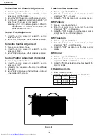
Vertical-Size and Linearity Adjustments

1. Receive a good local channel.
2. Enter the service mode and select the service

adjustment "D03" for V-size.

3. Adjust the "D03" bus data to get the proper V-size.
4. For V-linearity adjustment, select data bus "D05" and

adjust to get the proper vertical linearity.
Note: Aging for 10 min before adjustment. After the

adjustment of V-center and V-size, re-
adjustment for this V-line.

Vertical Phase Adjustment

1. Enter the service mode and select the service

adjustment  "D01".

2. Adjust "D01" data value so that picture is centered.

Horizontal Position Adjustment

1. Receive a good local channel.
2. Enter the service mode and select the service

adjustment  "D02".

3. Adjust "D02" data value so that picture is centered.

Caption Position Adjustment (Horizontal)

1. Receive a good local channel.
2. Enter the service mode and select the service

adjustment "EX2".

3. A black text box appears on the screen. (see 

Figure

B. below)

4. Adjust "EX2" data value so that text box is positioned

in the center of the screen.

Horizontal-Size Adjustment

1. Receive a good local channel.
2. Enter the service mode and select the service

adjustment "D04" for H-size.

3. Adjust the "D04" bus data to get the proper H-size.

EW-Parabola

1. Receive a good local channel.
2. Enter the service mode and select the service

adjustment "D07" for EW parabola.

3. Adjust the "D07" bus data to get the proper vertical

straight line for both left and right side.

EW-Trapezium

1. Receive a good local channel.
2. Enter the service mode and select the service

adjustment "D08" for EW-Trapezium.

3. Adjust the "D08" bus data to get the best position

display.

EW-Corner

1. Receive a good local channel.
2. Enter the service mode and select the service

adjustment "D09" for EW-Corner.

3. Adjust the "D09" bus data to get the best linearity for

4 corner points.

Other Adjustments

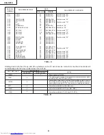
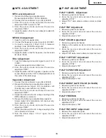
1. Enter the service mode.
2. Adjust the following data values as listed below.

SERVICE

ADJUST

DATA(Hex)

POSITION

ITEM

OP1

OPTION1

F7

OP2

OPTION2

10

OP3

OPTION3

0C

Figure B.

Summary of Contents for 36US50

Page 1: ...HEMATIC DIAGRAMS 15 PRINTED WIRING BOARD ASSEMBLIES 25 REPLACEMENT PARTS LIST 32 PACKING OF THE SET 42 CONTENTS SPEAKER SIZE 12 x 6 cm oval 2 pcs VOICE COIL IMPEDANCE 8 ohm at 400 Hz ANTENNA INPUT IMPEDANCE VHF UHF 75 ohm Unbalanced TUNING RANGES VHF Channels 2 thru 13 UHF Channels 14 thru 69 CATV Channels 1 thru 125 EIA Channel Plan U S A POWER INPUT 120V AC 60 Hz POWER RATING 167W PICTURE SIZE 3...

Page 2: ...de completely X RADIATION AND HIGH VOLTAGE LIMITS 1 Be sure all service personnel are aware of the procedures and instructions covering X radiation The only potential source of X ray in current solid state TV receivers is the picture tube However the picture tube does not emit measurable X Ray radiation if the high voltage is as specified in the High Voltage Check instructions It is only when high...

Page 3: ...ceed 0 5 milliamp Any measurements not within the limits outlined above indicate of a potential shock hazard and corrective action must be taken before returning the instrument to the customer 12345678901234567890123456789012123456789012345678901234567890121234567890123456789012345678901212 12345678901234567890123456789012123456789012345678901234567890121234567890123456789012345678901212 123456789...

Page 4: ... again Removes display Temporarily displays receiving channel when in Closed Caption mode INPUT Press Switch to external video INPUT 1 mode Press 2 times Switch to external video INPUT 2 mode Press 3 times Switch to external video INPUT 3 mode or COMPONENT mode Press 4 times Switch back to the original TV mode ENTER Used in some instances where a Cable Converter Box requires an enter command after...

Page 5: ...izontal oscillator does not stop in step 5 the circuit must be repaired before the set is returned to the customer HIGH VOLTAGE CHECK High voltage is not adjustable but must be checked to verify that the receiver is operating within safe and efficient design limitations as specified checks should be as follows 1 Connect an accurate high voltage meter between ground and anode of picture tube 2 Oper...

Page 6: ...s are in their proper reset position 2 Service number selection Once in the service mode press the Ch up or Ch down button on the remote controller or at the set The service adjustment number will vary in increments of one from V01 to P08 Select the item you wish to adjust 3 Data number selection Press the Vol up or Vol down button to adjust the data number To enter the service mode and exit serv ...

Page 7: ...RGB CONTRAST 20 0 63 00h 3Fh Must be set to 2A V32 Y DL 02 0 7 00h 07h Must be set to 02 V33 Y DL INPUT 01 0 7 00h 07h Must be set to 01 V34 VSM GAIN 07 0 7 00h 07h Must be set to 07 V35 N COMB 01 0 1 Must be set to 01 V36 BPF TOF INPUT 00 0 1 Must be set to 01 V37 CORING 00 0 1 Must be set to 00 V38 VSM PHASE 00 0 1 Must be set to 00 V39 COLOR γ 00 0 1 Must be set to 01 V40 SHARP INPUT 14 0 63 00...

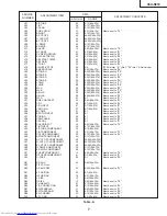
Page 8: ...5 HXA PIP 0A 0 255 00h FFh Must be set to 0A P06 HADJ PIP 00 0 15 00h 0Fh Must be set to 00 P07 FREE RUN PIP 0B 0 15 00h 0Fh Must be set to 0B P08 TINT PIP INPUT 24 0 63 00h 3Fh Must be set to 24 SERVICE NUMBER DATA ADJUSTMENT ITEM INITIAL VALUE RANGE ADJUSTMENT CONTENTS Table A NECESSARY UNNECESSARY ADJUSTMENT PART REPLACED IC2001 IC201 X Data is stored in IC2102 The adjustment is needed to compe...

Page 9: ...V03 and set to 00 minimum color Record original data code under adjustment V03 before changing V03 does not have to be adjusted if you selected a B W picture or monoscope pattern 3 Alternately adjust the service adjustment data of V09 and V10 until a good grey scale with normal whites is obtained RF Input 4 For component input the data value of V49 and V50 is adjusted to follow the data value of V...

Page 10: ...box appears on the screen see Figure B below 4 Adjust EX2 data value so that text box is positioned in the center of the screen Horizontal Size Adjustment 1 Receive a good local channel 2 Enter the service mode and select the service adjustment D04 for H size 3 Adjust the D04 bus data to get the proper H size EW Parabola 1 Receive a good local channel 2 Enter the service mode and select the servic...

Page 11: ...mposite signal Monaural signal 400Hz 100 modulation 2 Connect the rms voltmeter to pin 39 of IC3001 3 Enter the service mode and select the service adjustment M01 and set to 09 4 Enter the service mode and select the service adjustment EX4 5 Adjust the data so that the rms voltmeter reads 490 10 mVrms MTS VCO Adjustment 1 Keep the unit in no signal state 2 Connect the frequency counter to pin 39 o...

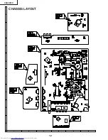
Page 12: ...36U S610 6 5 4 3 2 1 A B C D E F G H 12 CHASSIS LAYOUT ...

Page 13: ...36U S610 6 5 4 3 2 1 A B C D E F G H 13 BLOCK DIAGRAM ...

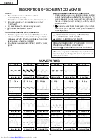
Page 14: ...trol 2 indicates waveform check points See chart waveforms are measured from point indicated to chassis ground å AND SHADED COMPONENTS SAFETY RELATED PARTS ç MARK X RAY RELATED PARTS DRGANNES MARQUES åET HACHRES PIECES RELATIVES A LA SECURITE MARQUE ç PIECS RELATIVE AUX RAYONS X This circuit diagram is a standard one printed circuits may be subject to change for product improvement without prior n...

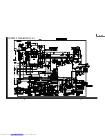
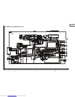
Page 15: ...36U S610 16 15 12 11 10 9 8 7 6 5 4 3 2 1 A B C D E F G H SCHEMATIC DIAGRAM MAIN 1 Unit ...

Page 16: ...12 11 10 9 8 7 6 5 4 3 2 1 A B C D E F G H SCHEMATIC DIAGRAM MAIN 2 Unit 36U S610 18 17 ...

Page 17: ...6 5 4 3 2 1 A B C D E F G H 19 SCHEMATIC DIAGRAM CRT Unit ...

Page 18: ...36U S610 21 20 12 11 10 9 8 7 6 5 4 3 2 1 A B C D E F G H SCHEMATIC DIAGRAM AV Unit ...

Page 19: ...36U S600 23 22 12 11 10 9 8 7 6 5 4 3 2 1 A B C D E F G H SCHEMATIC DIAGRAM P IN P Unit ...

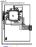
Page 20: ...36U S600 6 5 4 3 2 1 A B C D E F G H 24 SCHEMATIC DIAGRAM MTS MODULE Unit ...

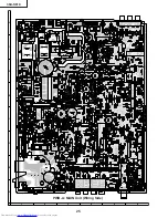
Page 21: ...36U S610 6 5 4 3 2 1 A B C D E F G H 25 PWB A MAIN Unit Wiring Side ...

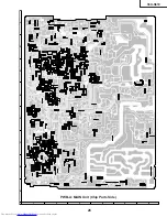
Page 22: ...36U S610 6 5 4 3 2 1 A B C D E F G H 26 PWB A MAIN Unit Chip Parts Side ...

Page 23: ...27 6 5 4 3 2 1 A B C D E F G H 36U S610 PWB B CRT Unit Wiring Side ...

Page 24: ...36U S610 6 5 4 3 2 1 A B C D E F G H 28 PWB C AV Unit Wiring Side PWB C AV Unit Chip Parts Side ...

Page 25: ...36U S610 6 5 4 3 2 1 A B C D E F G H 29 PWB R P IN P Unit Wiring Side PWB R P IN P Unit Chip Parts Side ...

Page 26: ...36U S610 6 5 4 3 2 1 A B C D E F G H 30 PWB S MTS MODULE Unit Wiring Side PWB S MTS MODULE Unit Chip Parts Side ...

Page 27: ...31 6 5 4 3 2 1 A B C D E F G H 36U S610 PWB F CONTROL Unit Wiring Side PWB F CONTROL Unit Component Side ...

Page 28: ... 2PD601AR AB Q601 VS2SC2482 1 J 2SC2482 AD å Q602 VS2SC5450 1E 2SC5450 or VS2SC5150 Q616 VS2PD601AR 1 J 2PD601AR AB Q634 VS2SC3198 G 1 J 2SC3198 G AA Q650 VS2SA1266 Y 1 J 2SA1266 Y AA Q672 VS2SA1266 Y 1 J 2SA1266 Y AA Q673 VS2SD2045 1 J 2SD2045 AL å Q701 VSST9NC60FP1E ST9NC60FP or VSST10NK60F Q727 VS2SC3333 1 J 2SC3333 AG Q728 VS2SA1091 01A J 2SA1091 01 AA Q729 VS2SA1266 Y 1 J 2SA1266 Y AA Q730 VS...

Page 29: ...amic Filter AD CF403 RFiLC0446CEZZ J Ceramic Filter AD CF2040 RFiLA0099CEZZ J Ceramic Filter AE SF201 RFiLC0405CEZZ J SAW Filter AH L51 VP CF270K0000 J Peaking 27µH AB L201 VP XF1R2K0000 J Peaking 1 2µH AB L203 VP DF100K0000 J Peaking 10µH AB L401 VP XF100K0000 J Peaking 10µH AB L642 RCiLZ1027CEZZ J Coil or RCiLZ0798CEZZ L671 RCiLZ1005CEZZ J Coil AH å L701 RCiLFA010WJZZ J Coil or RCiLFA313WJZZ or ...

Page 30: ... C706 RC KZ021SCEZZ J 3300p 2kV Ceramic AE C710 RC KZ0040CEZZ J 820p 2kV Ceramic AD C711 RC KZ021SCEZZ J 3300p 2kV Ceramic AE C712 VCKYCY1HB103K J 0 01 50V Ceramic AA C717 RC KZ0029CEZZ J 0 01 500V Ceramic AC C722 VCQYTA1HM104J J 0 1 50V Mylar AA C723 RC EZ0724CEZZ J 100 160V EL AG C725 RC EZ0810CEZZ J 330 160V EL AH or RC EZ1171CEZZ C726 VCKYPH3DB561K J 560p 2kV Ceramic AC C727 VCKYPH3DB561K J 56...

Page 31: ...1 16W M Ox AA R365 VRS CY1JF561J J 560 1 16W M Ox AA R367 VRN RL3DBR56J 0 56 2W M Film R368 VRD RA2BE222J J 2 2k 1 8W Carbon AA R369 VRD RA2BE822J J 8 2k 1 8W Carbon AA R370 VRS CY1JF122J J 1 2k 1 16W M Ox AA R371 VRS CY1JF102J J 1k 1 16W M Ox AA R372 VRS CY1JF223J J 22k 1 16W M Ox AA R415 VRS CY1JF101J J 100 1 16W M Ox AA R430 VRD RA2BE331J J 330 1 8W Carbon AA R431 VRS CY1JF331J J 330 1 16W M Ox...

Page 32: ... M Ox AA R906 VRS CY1JF392J J 3 9k 1 16W M Ox AA R907 VRS CY1JF182J J 1 8k 1 16W M Ox AA R909 VRS CY1JF102J J 1k 1 16W M Ox AA R910 VRD RA2BE102J J 1k 1 8W Carbon AA R911 VRS CY1JF683J J 68k 1 16W M Ox AA R912 VRS CY1JF223J J 22k 1 16W M Ox AA R913 VRS CY1JF392J J 3 9k 1 16W M Ox AA R914 VRS CY1JF182J J 1 8k 1 16W M Ox AA R915 VRS CY1JF102J J 1k 1 16W M Ox AA R916 VRS CY1JF683J J 68k 1 16W M Ox AA...

Page 33: ...Holder AB LX BZ3049GEFD J Screw AA LX BZ3100CEFD J Screw AA LX HZ3007MEFD J Screw PWB B DUNTKA527WEB3 CRT UNIT INTEGRATED CIRCUIT å IC850 VHiTDA6103Q 1 J TDA6103Q N3 AL TRANSISTORS Q850 VS2SA1266 Y 1 J 2SA1266 Y AA Q851 VS2SC3198 G 1 J 2SC3198 G AA DIODES D850 RH DX0220CEZZ J Diode AB D851 RH DX0220CEZZ J Diode AB D852 RH DX0220CEZZ J Diode AB D853 RH EX0647GEZZ J Zener Diode 15V AA or RH EX0417GE...

Page 34: ...W105M J 1 50V EL AB C1912 VCEA0A1HW105M J 1 50V EL AB C1913 VCEA0A1HW105M J 1 50V EL AB C1914 VCKYCY1HB681K J 680p 50V Ceramic AA C1915 VCKYCY1HF103Z J 0 01 50V Ceramic AA C1916 VCKYCY1HF103Z J 0 01 50V Ceramic AA C1921 VCKYCY1HB681K J 680p 50V Ceramic AA C1922 VCKYCY1CF104Z J 0 1 16V Ceramic AA C1923 VCEA0A1CW477M J 470 16V EL AC C1926 VCEA0A1CW226M J 22 16V EL AB C1927 VCKYCY1HB681K J 680p 50V C...

Page 35: ...H AB L1821 VP XF100K0000 J Peaking 10µH AB L1861 VP XF100K0000 J Peaking 10µH AB L1862 VP XF100K0000 J Peaking 10µH AB L1863 VP XF100K0000 J Peaking 10µH AB CAPACITORS EL Electrolytic C1721 VCE9GA1HW106M J 10 50V EL N P AB C1722 VCCCCY1HH330J J 33p 50V Ceramic AA C1741 VCQYTA1HM473J J 0 047 50V Mylar AA C1742 VCEA0A1HW105M J 1 50V EL AB C1743 VCQYTA1HM472J J 4700p 50V Mylar AB C1761 VCQYTA1HM473J ...

Page 36: ...J J 390 1 16W M Ox AA R1861 VRS CY1JF153J J 15k 1 16W M Ox AA R1862 VRS CY1JF102J J 1k 1 16W M Ox AA R1863 VRS CY1JF102J J 1k 1 16W M Ox AA R1864 VRS CY1JF221J J 220 1 16W M Ox AA R1865 VRS CY1JF474J J 470k 1 16W M Ox AA R1866 VRS CY1JF104J J 100k 1 16W M Ox AA R1867 VRS CY1JF202J J 2 0k 1 16W M Ox AA R1868 VRS CY1JF510J J 51 1 16W M Ox AA R1871 VRS CY1JF000J J 0 1 16W M Ox AA R1881 VRS CY1JF473J ...

Page 37: ...onnecting Cord GBN AC TCAUH3048GJZZ Caution Label AB TLABM0002GJZZ X Model Label AB TLABZ0152GJZZ X Feature Label AD XTASD30P12000 J Screw AA XTASD40P20000 J Screw AA SPAKCA105WEH0 Packing Case SPAKP0113GJZZ Wrapping Paper SPAKX0129GJZZ Buffer Material SSAKA0101GJZZ Polyethylene Bag TLABZ0152GJZZ Packing Label SUPPLIED ACCESSORIES PACKING PARTS NOT REPLACEMENT ITEM RRMCGA036WJSB Infrared R C Unit ...

Page 38: ... Case MARK Not replacement items FRONT Buffer Material Polyethylene Sheet Polyethylene Bag Operation Manual Infrared R C Unit Batteries REAR Use tape to fix the top side of packing case Use 12 staples to fix the bottom side of packing case ...

Page 39: ...a retrieval system or transmitted in any form or by any means electronic mechanical photocopying recording or otherwise without prior written permission of the publisher SHARP CORPORATION AV Systems Group Quality Reliability Control Center Yaita Tochigi 329 2193 Japan D SEM P SEMEX TQ0000 S May 2002 Printed in Japan MI KG ...

Reviews: