– 3 –
OUTLINE OF CIRCUIT DESCRIPTION
1-1. CMOS CIRCUIT DESCRIPTION
1. IC Configuration
The CMOS peripheral circuit block basically consists of the
following ICs.
IC911 (IMX039LQR) CMOS imager
H driver, V driver, serial communication circuit built-in
CDS/PGA built-in Gain + 18 dB (step pitch 0.1 dB)
10 bit/12 bit A/D converter built-in
2. IC911 (CMOS)
[Structure]
The electric charges which are generated when each pixel is
optically converted are in turn converted into signal voltages
by the FD amplifier, and they are then transmitted by the built-
in H driver and V driver. The signals are sampled and ampli-
fied by the CDS and PGA circuits at the point they are output,
and then they are AD converted and output. The output uses
the LVDS interface.
CMOS image sensor
Image size: diagonal 7.63 mm (1/2.3 type)
Pixels in total:
3632 (H) x 2832 (V) approx. 10.29 million pixels
Effective pixels:
-when using 1/2.3 type approx 9.29 million pixels:
3528 (H) x 2632 (V) approx. 9.29 million pixels
-when using 1/2.5 type approx 8.30 million pixels:
3336 (H) x 2488 (V) approx. 8.30 million pixels
-when using 1/2.9 type approx 5.56 million pixels:
3144 (H) x 1768 (V) approx. 5.56 million pixels
-when using 1/4.1 type approx 2.89 million pixels:
2160 (H) x 1336 (V) approx. 2.89 million pixels
Unit cell size: 1.75
µ
m (H) x 1.75
µ
m (V)
Optical black:
Horizontal (H) direction: Front 48 pixels, Rear 0 pixel
Vertical (V) direction:
Front 4 pixels, Rear 0 pixel
Summary of Contents for VPC-FH1BK - Xacti Camcorder - 1080p
Page 11: ... 11 MEMO ...
Page 27: ... 27 MEMO ...
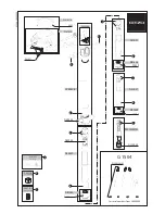
Page 29: ...29 1 2 3 4 5 6 7 8 9 10 13 14 11 12 ...
Page 64: ......