


YH1
HAP
(= @
-
@
YH1 + ,B•HAP
AGC CONT
t i
-:r-
1 I
R-Y
YH1
------n-----1--
1 I
I I
I
--+r:l
I I
I I
I I
I I
) �
I I
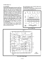
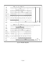
Fig. 2-12. H Aperture Correction
FADER MODE
FADE + DATE
(CONTROL VOLTAGE)
Fig. 2-1 1 . IC91 2 Block Diagram
2-5-2. C Slgnal Processing
The R-Y and B-Y signals from Pins CD and @ are clamped,
a burst flag pulse is added to them, and then they pass
through the sub-carrier modulation and blanking circuits
respectively, after which they are added to each other and
level controlled at the GC block.
At the GC block, the C signal is output from Pin @ after
being suppressed at the high luminance section and the
vertical edge by CSY (Pin ®
)
,
suppressed at low illumi
nation by the AGC voltage (Pin @
)
and attenuated by the
FADE voltage as the Y signal. After being band limited by
the external BPF, the C signal is input to Pin @ again, and
is fed from Pin @ to the VTR as CAM .C after being
amplified.
- 4-1 7 -


