though the adjustment is performed in VCR
record mode.
So you have to do it carefully.
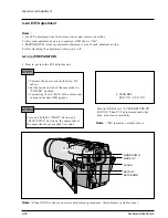
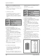
a. Preparations
b. Connect a power source.
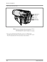
c. Get into the VCR adjustment mode.
d. Press the “FADE(MODE UP)” or “BLC(MODE
DOWN)” button of FUNCTION so as to select
the address 0B.
e. Insert a NORMAL Tape to the camcorder.
f. Press the “START/STOP” button on the Rear
board so as to set the camcorder to RECORD-
ING mode.
g. Record for enough time to check the waveform
when you playback where you recorded in
step f).
* 1 minute may be enough to check the waveform
in playback mode.
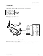
h. Connect the oscilloscope to the addressed Test
Point.
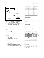
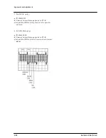
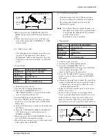
i. Make sure that the waveform is to be as typical
wave form on the next page.
(If OK, go to step l).
j. In case of the waveform level is bigger than
1Vp-p, press the Data Down button so as to set
to down the waveform level and if the wave-
form level smaller than 1Vp-p, press the Data
Up button so as to set to up the waveform level.
k. Repeat step g), h), i).
14
12
10
8
6
4
2
13
11
9
7
5
3
1
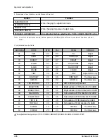
13
VIDEO OUT
12
11
10
9
8
7
6
5
4
3
2
1
NC
PB RF
AUDIO OUT
HD SW
VCR UNREG
JIG CS
VCR UNREG
JIG SCK
SS GND
JIG SO
JIG DETECT
JIG SI
VIDEO GND
14
CN452
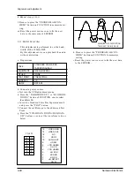
h. Be sure to press the “PROGRAM AE(CON-
FIRM)” button on FUNCTION to memorize
setting.
i. Reset the power source so as to fix the new data
to the camcorder’s EEPROM.
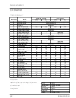
2-9. Y-FM Carrier (NOR)
: This adjustment is performed to set the sync-
tip level of the composite video signal.
Maladjusted Y-FM carrier impact to the play-
back picture, there may be black or white dot
noise.
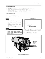
a. Preparations
b. Connect a power source.
c. Get into the VCR adjustment mode.
d. Press the “FADE(MODE UP)” “BLC (MODE
DOWN)” button of FUNCTION so as to select
the address 0A.
e. Insert a Normal Tape to the camcorder.
f. Press the “START/STOP” button on the Rear
board so as to set the camcorder to RECORD-
ING mode.
g. Connect the frequency counter to the addressed
Test Point.
h. Press the “TITLE(DATA DOWN)/ DSE(DATA
UP)” button so as to set the frequency to
4.38MHz±0.02MHz.
i. Be sure to press the “PROGRAM AE(CON-
FIRM)” button of FUNCTION to memorize set-
ting.
j. Reset the power source so as to fix the new data
to the camcorder’s EEPROM.
2-10. Y-FM DEVIATION (NOR)
: This adjustment sets the Y-FM modulation
level in recording. For adjustment, playback
the self-recorded signal and observe the
VIDEO OUT signal.
* Note : It is a little difficult to adjust because you
can check the waveform in playback mode even
Samsung Electronics
4-46
Alignment and Adjustment
TAPE
NORMAL TAPE FOR RECORDING
OSCILLOSCOPE
NONE
IC201 PIN41
0A
Y-FM CARRIER (NOR)
EQUIPMENT
OTHER
TEST POINT
ADDRESS
NAME
TAPE
NORMAL TAPE FOR RECORDING
OSCILLOSCOPE
NONE
CN452 PIN13
0B
Y-FM DEVIAT (NOR)
EQUIPMENT
OTHER
TEST POINT
ADDRESS
NAME
Summary of Contents for SCL500
Page 1: ...SERVICE MANUAL SAMSUNG VPL500 MODEL ...
Page 7: ...MEMO MEMO Products Specifications and Comparison Chart Samsung Electronics 2 4 ...
Page 85: ...Samsung Electronics 5 18 Exploded View and Parts List MEMO MEMO ...
Page 115: ...7 2 Samsung Electronics PCB Diagrams 7 1 Main PCB Normal Component Side ...
Page 116: ...7 3 Samsung Electronics PCB Diagrams ...
Page 117: ...7 4 Samsung Electronics PCB Diagrams 7 2 Main PCB Normal Conductor Side ...
Page 118: ...7 5 Samsung Electronics PCB Diagrams ...
Page 119: ...7 6 Samsung Electronics PCB Diagrams 7 3 Main PCB Hi8 Component Side ...
Page 120: ...7 7 Samsung Electronics PCB Diagrams ...
Page 121: ...7 8 Samsung Electronics PCB Diagrams 7 4 Main PCB Hi8 Conductor Side ...
Page 122: ...7 9 Samsung Electronics PCB Diagrams ...
Page 124: ...7 11 Samsung Electronics PCB Diagrams 7 6 CCD PCB Component Side Conductor Side ...
Page 125: ...7 12 Samsung Electronics PCB Diagrams 7 7 CVF PCB Component Side Conductor Side ...
Page 126: ...7 13 Samsung Electronics PCB Diagrams 7 8 EVF PCB Component Side Conductor Side ...
Page 127: ...7 14 Samsung Electronics PCB Diagrams 7 9 Function PCB Component Side Conductor Side ...
Page 128: ...7 15 Samsung Electronics PCB Diagrams 7 10 LCD PCB Component Side Conductor Side ...
Page 129: ...7 16 Samsung Electronics PCB Diagrams 7 11 Front PCB ...
Page 130: ...8 1 Samsung Electronics 8 Wiring Diagram ...
Page 131: ...8 2 Samsung Electronics Wiring Diagram MEMO MEMO ...
Page 135: ...9 4 Samsung Electronics Schematic Diagrams 9 1 DC DC Converter Main ...
Page 136: ...9 5 Samsung Electronics Schematic Diagrams 9 2 System Control Servo Main ...
Page 137: ...9 6 Samsung Electronics Schematic Diagrams 9 3 Video Normal Main ...
Page 138: ...9 7 Samsung Electronics Schematic Diagrams 9 4 Video Hi8 Main ...
Page 139: ...9 8 Samsung Electronics Schematic Diagrams 9 5 Audio Main ...
Page 140: ...9 9 Samsung Electronics Schematic Diagrams 9 6 Camera Main ...
Page 141: ...9 10 Samsung Electronics Schematic Diagrams 9 7 Rear ...
Page 142: ...9 11 Samsung Electronics Schematic Diagrams 9 8 CCD ...
Page 143: ...9 12 Samsung Electronics Schematic Diagrams 9 9 CVF ...
Page 144: ...9 13 Samsung Electronics Schematic Diagrams 9 10 Front ...
Page 145: ...9 14 Samsung Electronics Schematic Diagrams 9 11 Function ...
Page 146: ...9 15 Samsung Electronics Schematic Diagrams 9 12 EVF ...
Page 147: ...9 16 Samsung Electronics Schematic Diagrams 9 13 LCD ...

