Samsung Electronics
4-31
Alignment and Adjustment
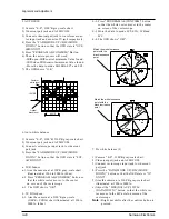
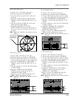
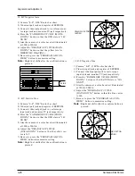
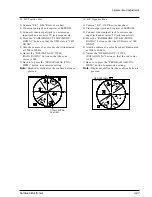
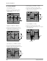
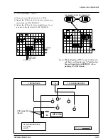
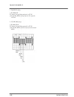
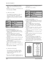
6. TINT(ADDRESS : 0.TINT)
1) Connect an oscilloscope probe to TP-B.
2) Adjust the EVR so that the dual waveforms are
superimposed.(PAL MODEL)
3) Adjust the EVR so that the bright(Green) level
is equal to the Red level.(NTSC MODEL)
DUAL WAVEFORMS ARE SUPERIMPOSED.
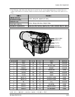
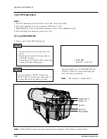
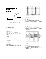
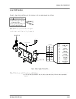
ADJ. point
1. PLL
3. R-SUB BRIGHTNESS
2. BRIGHTNESS
10P CON
4. B-SUB BRIGHTNESS
5. COLOR
6. HUE
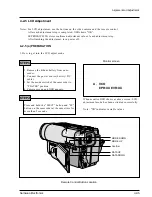
Note : When adjusting CVF be sure to short cir-
cuit between Ground and “A”part to store
the confirmed data in EEPROM when
pushing ON/OFF button.
A
GND
G
R
B
P
L
CVF Adjust Mode
(Short)
YELLOW LEVEL
PEDESTAL
LINE
GREEN LEVEL
RED LEVEL
Summary of Contents for SCL500
Page 1: ...SERVICE MANUAL SAMSUNG VPL500 MODEL ...
Page 7: ...MEMO MEMO Products Specifications and Comparison Chart Samsung Electronics 2 4 ...
Page 85: ...Samsung Electronics 5 18 Exploded View and Parts List MEMO MEMO ...
Page 115: ...7 2 Samsung Electronics PCB Diagrams 7 1 Main PCB Normal Component Side ...
Page 116: ...7 3 Samsung Electronics PCB Diagrams ...
Page 117: ...7 4 Samsung Electronics PCB Diagrams 7 2 Main PCB Normal Conductor Side ...
Page 118: ...7 5 Samsung Electronics PCB Diagrams ...
Page 119: ...7 6 Samsung Electronics PCB Diagrams 7 3 Main PCB Hi8 Component Side ...
Page 120: ...7 7 Samsung Electronics PCB Diagrams ...
Page 121: ...7 8 Samsung Electronics PCB Diagrams 7 4 Main PCB Hi8 Conductor Side ...
Page 122: ...7 9 Samsung Electronics PCB Diagrams ...
Page 124: ...7 11 Samsung Electronics PCB Diagrams 7 6 CCD PCB Component Side Conductor Side ...
Page 125: ...7 12 Samsung Electronics PCB Diagrams 7 7 CVF PCB Component Side Conductor Side ...
Page 126: ...7 13 Samsung Electronics PCB Diagrams 7 8 EVF PCB Component Side Conductor Side ...
Page 127: ...7 14 Samsung Electronics PCB Diagrams 7 9 Function PCB Component Side Conductor Side ...
Page 128: ...7 15 Samsung Electronics PCB Diagrams 7 10 LCD PCB Component Side Conductor Side ...
Page 129: ...7 16 Samsung Electronics PCB Diagrams 7 11 Front PCB ...
Page 130: ...8 1 Samsung Electronics 8 Wiring Diagram ...
Page 131: ...8 2 Samsung Electronics Wiring Diagram MEMO MEMO ...
Page 135: ...9 4 Samsung Electronics Schematic Diagrams 9 1 DC DC Converter Main ...
Page 136: ...9 5 Samsung Electronics Schematic Diagrams 9 2 System Control Servo Main ...
Page 137: ...9 6 Samsung Electronics Schematic Diagrams 9 3 Video Normal Main ...
Page 138: ...9 7 Samsung Electronics Schematic Diagrams 9 4 Video Hi8 Main ...
Page 139: ...9 8 Samsung Electronics Schematic Diagrams 9 5 Audio Main ...
Page 140: ...9 9 Samsung Electronics Schematic Diagrams 9 6 Camera Main ...
Page 141: ...9 10 Samsung Electronics Schematic Diagrams 9 7 Rear ...
Page 142: ...9 11 Samsung Electronics Schematic Diagrams 9 8 CCD ...
Page 143: ...9 12 Samsung Electronics Schematic Diagrams 9 9 CVF ...
Page 144: ...9 13 Samsung Electronics Schematic Diagrams 9 10 Front ...
Page 145: ...9 14 Samsung Electronics Schematic Diagrams 9 11 Function ...
Page 146: ...9 15 Samsung Electronics Schematic Diagrams 9 12 EVF ...
Page 147: ...9 16 Samsung Electronics Schematic Diagrams 9 13 LCD ...

