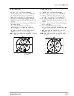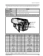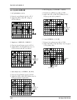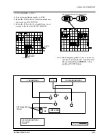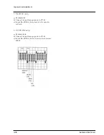
Samsung Electronics
4-28
Alignment and Adjustment
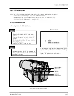
4-2-3 CVF Adjustment
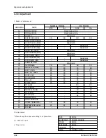
Notes :
1. After each adjustment step is completed, OSD shows “OK”.
2. EEPROM(ICV02) stores confirmed adjustment value of each adjustment step.
3. After finishing the adjustment, reset the main power source (OFF-ON) to memorize the adjustment data
in EEPROM.
4. Remote controller is used as a CVF adjust tool.
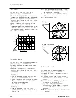
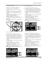
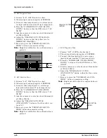
4-2-3 (a) PREPARATION
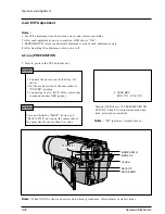
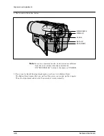
1. How to get into the CVF adjust mode.
Note : When XX XX is shown in service adjustment procedures, this indicates variable values.
1. Connect the power source (battery/DC
cable).
2. Set the mode switch of the camcorder to
“PLAYER” position.
3. Set OSD on state.
4. Press and hold the “EJECT” button and
“PLAY/STILL” button on the camcorder at
the same time for more than 5 seconds.
Then unit goes into service mode.
STEP2
MONITOR OSD shows “8. PLL EPR XX.
EVR XX”. Then CVF adjustment mode has
been activated successfully.
STEP3
8 PLL
EPR : XX EVR : XX
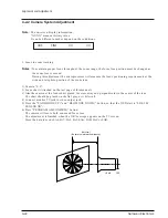
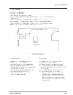
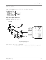
Short the two lands on the CVF PCB by sol-
der to Ground. (They are displayed on page
4-31)
STEP1
EJECT
MODE DOWN
MODE UP
Confirm
DATA UP
DATA DOWN
PLAY/STILL
Summary of Contents for SCL500
Page 1: ...SERVICE MANUAL SAMSUNG VPL500 MODEL ...
Page 7: ...MEMO MEMO Products Specifications and Comparison Chart Samsung Electronics 2 4 ...
Page 85: ...Samsung Electronics 5 18 Exploded View and Parts List MEMO MEMO ...
Page 115: ...7 2 Samsung Electronics PCB Diagrams 7 1 Main PCB Normal Component Side ...
Page 116: ...7 3 Samsung Electronics PCB Diagrams ...
Page 117: ...7 4 Samsung Electronics PCB Diagrams 7 2 Main PCB Normal Conductor Side ...
Page 118: ...7 5 Samsung Electronics PCB Diagrams ...
Page 119: ...7 6 Samsung Electronics PCB Diagrams 7 3 Main PCB Hi8 Component Side ...
Page 120: ...7 7 Samsung Electronics PCB Diagrams ...
Page 121: ...7 8 Samsung Electronics PCB Diagrams 7 4 Main PCB Hi8 Conductor Side ...
Page 122: ...7 9 Samsung Electronics PCB Diagrams ...
Page 124: ...7 11 Samsung Electronics PCB Diagrams 7 6 CCD PCB Component Side Conductor Side ...
Page 125: ...7 12 Samsung Electronics PCB Diagrams 7 7 CVF PCB Component Side Conductor Side ...
Page 126: ...7 13 Samsung Electronics PCB Diagrams 7 8 EVF PCB Component Side Conductor Side ...
Page 127: ...7 14 Samsung Electronics PCB Diagrams 7 9 Function PCB Component Side Conductor Side ...
Page 128: ...7 15 Samsung Electronics PCB Diagrams 7 10 LCD PCB Component Side Conductor Side ...
Page 129: ...7 16 Samsung Electronics PCB Diagrams 7 11 Front PCB ...
Page 130: ...8 1 Samsung Electronics 8 Wiring Diagram ...
Page 131: ...8 2 Samsung Electronics Wiring Diagram MEMO MEMO ...
Page 135: ...9 4 Samsung Electronics Schematic Diagrams 9 1 DC DC Converter Main ...
Page 136: ...9 5 Samsung Electronics Schematic Diagrams 9 2 System Control Servo Main ...
Page 137: ...9 6 Samsung Electronics Schematic Diagrams 9 3 Video Normal Main ...
Page 138: ...9 7 Samsung Electronics Schematic Diagrams 9 4 Video Hi8 Main ...
Page 139: ...9 8 Samsung Electronics Schematic Diagrams 9 5 Audio Main ...
Page 140: ...9 9 Samsung Electronics Schematic Diagrams 9 6 Camera Main ...
Page 141: ...9 10 Samsung Electronics Schematic Diagrams 9 7 Rear ...
Page 142: ...9 11 Samsung Electronics Schematic Diagrams 9 8 CCD ...
Page 143: ...9 12 Samsung Electronics Schematic Diagrams 9 9 CVF ...
Page 144: ...9 13 Samsung Electronics Schematic Diagrams 9 10 Front ...
Page 145: ...9 14 Samsung Electronics Schematic Diagrams 9 11 Function ...
Page 146: ...9 15 Samsung Electronics Schematic Diagrams 9 12 EVF ...
Page 147: ...9 16 Samsung Electronics Schematic Diagrams 9 13 LCD ...

