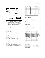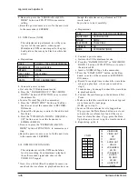
d. Press the “FADE(MODE UP)” or
“BLC(MODE DOWN)” button of FUNCTION
so as to select the address 07.
e. Insert the Hi-8 tape to the camcorder
f. Connect the oscilloscope to the addressed Test
Point.
g. “TITLE(DATA DOWN)/DSE(DATA UP)” but-
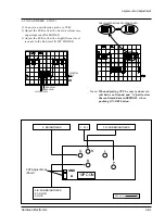
ton so that the IC201 PIN13 is 0.5±0.02Vp-p
from SYNC tip to peak level.
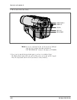
h. Be sure to press the “PROGRAM AE(CON-
FIRM)” button on FUNCTION to memorize
setting.
i. Reset the power source so as to fix the new data
to the camcorder’s EEPROM.
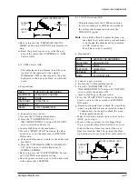
2-7. PB Output Level (Hi8)
: This adjustment is performed to set the A/D
input level to the regulated level.
a. Preparations
b. Connect a power source.
c. Get into the VCR adjustment mode.
d. Press the “FADE(MODE UP)” or “BLC (MODE
DOWN)” button of FUNCTION so as to select
the address 08.
e. Insert a Hi-8 standard color bar tape and press
the PLAY button.
f. Connect the oscilloscope counter to the
addressed Test Point.
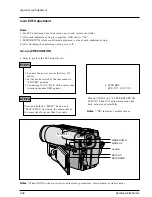
g. Press the “TITLE(DATA DOWN)/DSE(DATA
UP)” button so that the CN452 PIN13 is
0.9±0.02Vp-p from SYNC to peak level.
h. Be sure to press the “PROGRAM AE(CON-
FIRM)” button on FUNCTION to memorize
setting.
i. Reset the power source so as to fix the new data
to the camcorder’s EEPROM.
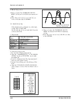
2-8. VIDEO Out Level
: This adjustment is performed to set the VIDEO
out level to the regulated level.
a. Preparations
b. Connect a power source.
c. Get into the VCR adjustment mode.
d. Press the “FADE(MODE UP)” “BLC (MODE
DOWN)” button of FUNCTION so as to select
the address 09.
e. Insert a standard color bar tape and press the
PLAY button.
f. Connect the oscilloscope counter to the
addressed Test Point.
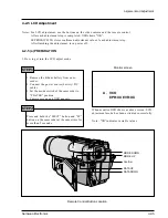
g. Press the “TITLE(DATA DOWN)/DSE(DATA
UP)” button so that the CN452 PIN13 is
1.0±0.02Vp-p from SYNC to peak level.
Samsung Electronics
4-45
Alignment and Adjustment
0.5 0.02Vp-p
TAPE
STANDARD COLOR BAR TAPE
RECORDED WITH SP SPEED
OSCILLOSCOPE
R248
06
PB OUT-LEVEL (NOR)
EQUIPMENT
TEST POINT
ADDRESS
NAME
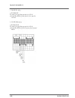
0.9 0.02Vp-p
TAPE
STANDARD COLOR BAR TAPE
RECORDED WITH SP SPEED
OSCILLOSCOPE
CONNET THE MOINTER(75
Ω
)
CN452 PIN13
09
VIDEO OUT LEVEL
EQUIPMENT
OTHER
TEST POINT
ADDRESS
NAME
APPROX.
0.7V
APPROX.
0.3V
WHITE ( APPROX. 100% )
H
1.0 0.02Vp-p
Summary of Contents for SCL500
Page 1: ...SERVICE MANUAL SAMSUNG VPL500 MODEL ...
Page 7: ...MEMO MEMO Products Specifications and Comparison Chart Samsung Electronics 2 4 ...
Page 85: ...Samsung Electronics 5 18 Exploded View and Parts List MEMO MEMO ...
Page 115: ...7 2 Samsung Electronics PCB Diagrams 7 1 Main PCB Normal Component Side ...
Page 116: ...7 3 Samsung Electronics PCB Diagrams ...
Page 117: ...7 4 Samsung Electronics PCB Diagrams 7 2 Main PCB Normal Conductor Side ...
Page 118: ...7 5 Samsung Electronics PCB Diagrams ...
Page 119: ...7 6 Samsung Electronics PCB Diagrams 7 3 Main PCB Hi8 Component Side ...
Page 120: ...7 7 Samsung Electronics PCB Diagrams ...
Page 121: ...7 8 Samsung Electronics PCB Diagrams 7 4 Main PCB Hi8 Conductor Side ...
Page 122: ...7 9 Samsung Electronics PCB Diagrams ...
Page 124: ...7 11 Samsung Electronics PCB Diagrams 7 6 CCD PCB Component Side Conductor Side ...
Page 125: ...7 12 Samsung Electronics PCB Diagrams 7 7 CVF PCB Component Side Conductor Side ...
Page 126: ...7 13 Samsung Electronics PCB Diagrams 7 8 EVF PCB Component Side Conductor Side ...
Page 127: ...7 14 Samsung Electronics PCB Diagrams 7 9 Function PCB Component Side Conductor Side ...
Page 128: ...7 15 Samsung Electronics PCB Diagrams 7 10 LCD PCB Component Side Conductor Side ...
Page 129: ...7 16 Samsung Electronics PCB Diagrams 7 11 Front PCB ...
Page 130: ...8 1 Samsung Electronics 8 Wiring Diagram ...
Page 131: ...8 2 Samsung Electronics Wiring Diagram MEMO MEMO ...
Page 135: ...9 4 Samsung Electronics Schematic Diagrams 9 1 DC DC Converter Main ...
Page 136: ...9 5 Samsung Electronics Schematic Diagrams 9 2 System Control Servo Main ...
Page 137: ...9 6 Samsung Electronics Schematic Diagrams 9 3 Video Normal Main ...
Page 138: ...9 7 Samsung Electronics Schematic Diagrams 9 4 Video Hi8 Main ...
Page 139: ...9 8 Samsung Electronics Schematic Diagrams 9 5 Audio Main ...
Page 140: ...9 9 Samsung Electronics Schematic Diagrams 9 6 Camera Main ...
Page 141: ...9 10 Samsung Electronics Schematic Diagrams 9 7 Rear ...
Page 142: ...9 11 Samsung Electronics Schematic Diagrams 9 8 CCD ...
Page 143: ...9 12 Samsung Electronics Schematic Diagrams 9 9 CVF ...
Page 144: ...9 13 Samsung Electronics Schematic Diagrams 9 10 Front ...
Page 145: ...9 14 Samsung Electronics Schematic Diagrams 9 11 Function ...
Page 146: ...9 15 Samsung Electronics Schematic Diagrams 9 12 EVF ...
Page 147: ...9 16 Samsung Electronics Schematic Diagrams 9 13 LCD ...

