Samsung Electronics
1-3
Precaution
1-2 Servicing Precautions
1. Servicing precautions are printed on the cabinet. Follow them.
2. Always unplug the unit’s AC power cord from the AC power source before attempting to: (a) Remove or reinstall
any component or assembly, (b) Disconnect an electrical plug or connector, (c) Connect a test component in
parallel with an electrolytic capacitor.
3. Some components are raised above the printed circuit board for safety. An insulation tube or tape is sometimes
used. The internal wiring may be clamped to prevent contact with thermally hot components. Reinstall all such
elements to their original position.
4. After servicing, always check that the screws, components and wiring have been correctly reinstalled.
Make sure that the portion around the serviced part has not been damaged.
5. Check the insulation between the blades of the AC plug and accessible conductive parts (examples: metal
panels, input terminals and earphone jacks).
6. Insulation Checking Procedure: Disconnect the power cord from the AC source. Connect an insulation
resistance meter (500V) to the blades of the AC plug.
The insulation resistance between each blade of the AC plug and accessible conductive parts (see above)
should be greater than 1 megohm.
7. Never defeat any of the B+ voltage interlocks. Do not apply AC power to the unit (or any of its assemblies)
unless all solid-state heat sinks are correctly installed.
8. Always connect a test instrument’s ground lead to the instrument chassis ground before connecting the positive
lead; always remove the instrument’s ground lead last.
First read the “Safety Precautions” section of this manual. If some unforeseen circumstance
creates a conflict between the servicing and safety precautions, always follow the safety
precautions.
Summary of Contents for HT-C553
Page 8: ...3 4 Samsung Electronics MEMO...
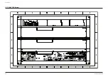
Page 23: ...6 2 Samsung Electronics PCB Diagram 6 2 FRONT PCB Top FCON1 UIC2 KIC2 U1 2 1...
Page 25: ...6 4 Samsung Electronics PCB Diagram 6 3 FRONT PCB Bottom...
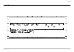
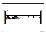
Page 26: ...Samsung Electronics 6 5 PCB Diagram 6 4 KEY PCB Top...
Page 27: ...6 6 Samsung Electronics PCB Diagram 6 5 KEY PCB Bottom CN1 IC1 1...
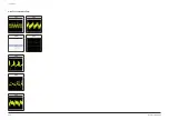
Page 31: ...6 10 Samsung Electronics PCB Diagram TP1 TP2 TP3 TP4 TP5 6 6 2 Test Point Wave Form TP6 TP7...
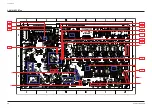
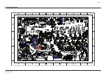
Page 33: ...6 12 Samsung Electronics PCB Diagram 6 8 SMPS PCB Top CON1...
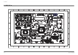
Page 34: ...Samsung Electronics 6 13 PCB Diagram 6 9 SMPS PCB Bottom CON2 CON3...
Page 35: ...6 14 Samsung Electronics MEMO...
Page 47: ...2 8 Samsung Electronics MEMO...


