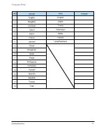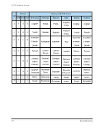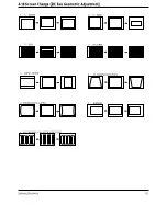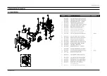
4-10
Samsung Electronics
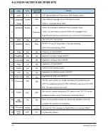
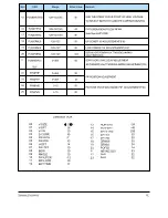
REMARK
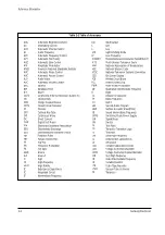
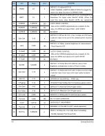
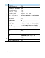
DDP3310 R,1AEhex BIT(7:5)
-USER PEAKING CONRTOL REDUCTION (The bigger the
value is the larger the amount of REDUCTION)
VPC3230 FP BLOCK R,52hex (BIT(7:0)), R,53hex(BIT(5:0))
Reproduce the levels under BLACK LEVEL (When the
level=1,the levels under BLACK LEVEL are reproduced)
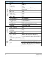
WHITE DRIVE CONTROL
- After all the SCREEN adjustments are complete, fix the
value of G DRIVE and adjust HIGH LIGHT WHITE
BALANCE.
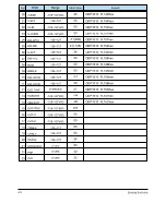
DDP3310 R,1B1hex Bit <5:0> (Use 12 steps out of 63 steps
to add the value of sub cont to the contrast control of picture
control)
DDP3310 R,168hex (Internal brightness for measurement)
- Fixed Value by CRT
CUTOFF DRIVE CONRTOL
- After all the SCREEN adjustments are complete, fix the
value of G DRIVE and adjust LOW LIGHT WHITE
BALANCE.
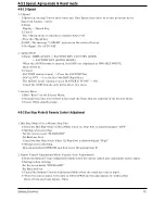
DDP3310 R,167hex Bit<15:6>(Add the value of Sub
Brightness to Brightness Control of Picture Control)
DDP3310 R,1B2hex Bit<15:9>(Use 12 steps out of 63 steps
to add the value of sub color to the color control of picture
control)
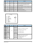
VPC3230 FP Sub R,DChex - NTSC only
VPC3230 FP Sub R,28hex Bit<11:8>(Vertical peaking control)
DDP3310 R,1A7hex Bit<5:0>(VM gain control)
DDP3310 R,19Bhex Bit<3:0>(VM gain control)
DDP3310 R,19FBhex Bit<7:0>(VM limit value control)
Set TTX mode conrtast level
DDP3310 EXT BRIGHTNESS
SDA9489X R,11hex Bit<7:4>(PIP contrast adjustment)
DD3310 R,160hex Bit <15:4>(ABL thresh hold setting)
- Set ABL Operation Point (Cuve Point)
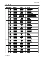
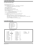
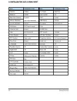
Item
00
01
02
03
04
05
06
07
08
09
10
11
12
13
14
15
16
17
18
19
20
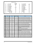
OS D
PKRD
BRCT
R DRIVE
B DRIVE
G DRIVE
Sub Cont
Lbrm
R Cutoff
B Cutoff
G Cutoff
Sub Brt.
Sub Color
Sub Tint
V Peaking
Svm Gain
Svm Delay
Svm Limit
Ttx Cont
Ttx brt
Pip Cont
Bcl Thrs
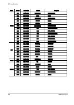
Range
0-7
0-1
0-255(X2)
0-255(X2)
0-255(X2)
0-12
0-255
0-255
0-255
0-255
0-20(X8)
0-12
0-12
0-12
0-63
0-15
0-255
0-255
-128-127
0-15
0-255(X8)
29A7
3
0
200
200
200
6
180
80
80
80
6
8
4
7
32
5
85
120
15
0
41
Summary of Contents for CS29A7HF9X/XSV
Page 2: ...ELECTRONICS Samsung Electronics Co Ltd May 2001 Printed in Korea 3KS4A P 2910...
Page 12: ...3 2 Samsung Electronics MEMO...
Page 36: ...4 24 Samsung Electronics MEMO...
Page 89: ...Samsung Electronics 7 Block Diagrams 7 1 Voltage Current Block...
Page 96: ...Schematic Diagrams 8 4 Samsung Electronics 8 3 MAIN 3 3 RCA Power Line Signal Line...
Page 98: ...8 5 MAIN 2 3 SCART Schematic Diagrams 8 6 Samsung Electronics TP19 TP20 TP21 TP19 TP20 TP21...
Page 99: ...Samsung Electronics 8 6 MAIN 3 3 SCART Schematic Diagrams 8 7...
Page 100: ...Schematic Diagrams 8 8 Samsung Electronics 8 7 MICOM...
Page 103: ...Samsung Electronics Schematic Diagrams 8 11 8 9 CRT SIDE A V CRT SIDE AV...
Page 104: ...Schematic Diagrams 8 12 Samsung Electronics 8 10 DOLBY...
Page 105: ...Samsung Electronics 8 11 F BOX 1 3 Schematic Diagrams 8 13...
Page 106: ...8 12 F BOX 2 3 Schematic Diagrams 8 14 Samsung Electronics...
Page 107: ...Samsung Electronics 8 13 F BOX 3 3 Schematic Diagrams 8 15...

