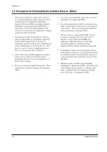
1. Some semiconductor (“solid state”) devices
are easily damaged by static electricity. Such
components are called Electrostatically
Sensitive Devices (ESDs); examples include
integrated circuits and some field-effect
transistors. The following techniques will
reduce the occurrence of component damage
caused by static electricity.
2. Immediately before handling any semicon
ductor components or assemblies, drain the
electrostatic charge from your body by
touching a known earth ground. Alternatively,
wear a discharging wrist-strap device. (Be
sure to remove it prior to applying power—
this is an electric shock precaution.)
3. After removing an ESD-equipped assembly,
place it on a conductive surface such as
aluminum foil to prevent accumulation of
electrostatic charge.
4. Do not use freon-propelled chemicals. These
can generate electrical charges that damage
ESDs.
5. Use only a grounded-tip soldering iron when
soldering or unsoldering ESDs.
6. Use only an anti-static solder removal device.
Many solder removal devices are not rated as
“anti-static”; these can accumulate sufficient
electrical charge to damage ESDs.
7. Do not remove a replacement ESD from its
protective package until you are ready to
install it. Most replacement ESDs are
packaged with leads that are electrically
shorted together by conductive foam,
aluminum foil or other conductive materials.
8. Immediately before removing the protective
material from the leads of a replacement ESD,
touch the protective material to the chassis or
circuit assembly into which the device will be
installed.
9. Minimize body motions when handling
unpackaged replacement ESDs. Motions such
as brushing clothes together, or lifting a foot
from a carpeted floor can generate enough
static electricity to damage an ESD.
Precautions
1-4
Samsung Electronics
1-3 Precautions for Electrostatically Sensitive Devices (ESDs)
Summary of Contents for CS29A7HF9X/XSV
Page 2: ...ELECTRONICS Samsung Electronics Co Ltd May 2001 Printed in Korea 3KS4A P 2910...
Page 12: ...3 2 Samsung Electronics MEMO...
Page 36: ...4 24 Samsung Electronics MEMO...
Page 89: ...Samsung Electronics 7 Block Diagrams 7 1 Voltage Current Block...
Page 96: ...Schematic Diagrams 8 4 Samsung Electronics 8 3 MAIN 3 3 RCA Power Line Signal Line...
Page 98: ...8 5 MAIN 2 3 SCART Schematic Diagrams 8 6 Samsung Electronics TP19 TP20 TP21 TP19 TP20 TP21...
Page 99: ...Samsung Electronics 8 6 MAIN 3 3 SCART Schematic Diagrams 8 7...
Page 100: ...Schematic Diagrams 8 8 Samsung Electronics 8 7 MICOM...
Page 103: ...Samsung Electronics Schematic Diagrams 8 11 8 9 CRT SIDE A V CRT SIDE AV...
Page 104: ...Schematic Diagrams 8 12 Samsung Electronics 8 10 DOLBY...
Page 105: ...Samsung Electronics 8 11 F BOX 1 3 Schematic Diagrams 8 13...
Page 106: ...8 12 F BOX 2 3 Schematic Diagrams 8 14 Samsung Electronics...
Page 107: ...Samsung Electronics 8 13 F BOX 3 3 Schematic Diagrams 8 15...

