background image

2 Product Specifications 

2-6 


SAM4S ER-600 SERIES


2-4 Interface Specifications


2-4-1 RS-232C Serial Interface 

2-4-1-(d) Signal Description     

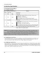
Pin No.  Signal Name 

Signal Direction 

Function 

BODY 

Frame GND 

Frame Ground 

  2 

RXD 

Input 

Receive Data 

  3 

TXD 

Output 

Transmit Data 

  4 

DTR 

Output 

This Signal indicates whether the ECR(Easy Cash) is busy. (H/W flow control) 


MARK(Logic1) : The ECR is busy 


SPACE(Logic0) : The ECR is not busy 


The host transmits a data to the ECR, after confirming this signal.   


When XON/XOFF flow control is selected, the host does not check this signal. 

  5 

Signal GND 

-     

Signal Ground 

  6 

DSR 

Input 

This signal indicates whether the host computer or receipt printer can receive data. 
(H/W flow control) 


MARK(Logic1) : The host can receive a data 


SPACE(Logic0) : The host can not receive a data 


The ECR transmits a data to the host or receipt printer, after confirming this signal.


When XON/XOFF flow control is selected, the printer does not check this signal.   

    9 

VCC 

Output 

VCC(+5V/200mA) is supplied at 9Pin of D-SUB Connector.(RS-232 #1,4) 

Table2-4 RS-232C Signal Description 


Caution: 

The VCC is supplied for the barcode or other devices power source. The Supply Current 200mA is total 
value including COM1 and COM4 Power Consumption. If the Total Power Consumption of the attached 
devices is exceeded the specification (200mA), the system stops the VCC of D-SUB Connector.   

Caution: 

If the device with 5V/200mA is connected to COM1, the VCC of COM4 can not use. If the device with 
5V/100mA is connected to COM1, Other device with 5V/100mA can be connected to COM4 Port. 

Caution:

  If you use the VCC of COM4 , you connect the switch at CN10(1,2pin). 


2-4-1-(e) H/W Flow Control Timing 

When DTR/DSR flow control is select, before transmitting a data, the ECR checks whether the host is BUSY or not.   
If the host is BUSY, ECR does not transmit a data to the host. If the host is not BUSY, ECR transmits a data to the   
Host. The host is the same. Refer to the Interface Part of Chapter 7(Special Circuit Diagrams).     


2-4-1-(f) S/W Flow Control Timing 

When XON/XOFF flow control is selected, the ECR transmits XON(ASCII 11h) or XOFF(ACSII 13h) signal    through 
the Serial Data Line.    If the ECR is busy, the printer transmits XOFF(ASCII 13h) to host through the Serial Data Line. 
Then the host recognizes that the ECR is busy.    So, the host does not transmit a data to the ECR. If the ECR is released 
from busy, the ECR transmits XON(ASCII 11h) to host through the Serial Data Line. Then the host recognizes that the 
ECR is not busy. And the host transmits a data to the ECR. 


Summary of Contents for ER-600

Page 1: ...ution Statements 2 Product Specifications 3 Installation and Operation 4 Disassembly and Assembly 5 Reference Information 6 Special Circuit Descriptions 7 Troubleshooting 8 Exploded Views and Parts Li...

Page 2: ...Electronic Cash Register Notes Notes may appear anywhere in the manual They describe additional information about the item Precaution symbols Indicates a Safety Precaution that applies to this part co...

Page 3: ...may not in whole or in part be copied photocopied reproduced translated or converted to any electronic or machine readable from without prior written permission of Shin Heung Precision SAM4S ER 600 SE...

Page 4: ...bleshooting All information in this manual is subject to change without prior notice Therefore you must check the correspondence of your manual with your machine No part of this manual may be copied o...

Page 5: ...dges and especially the AC and high voltage supplies Always inspect for pinched out of place or frayed wiring Do not change the spacing between comp onents and the printed circuit board Check the AC p...

Page 6: ...strument s ground lead to the instrument chassis ground before connecting the positive lead always remove the instrument s ground lead last 1 3 Precautions for Electrostatic Sensitive Devices ESDs 1 S...

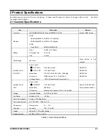
Page 7: ...ed Interface Serial RS 232C Flow Control DTR DSR H W Flow Control XON XOFF S W Flow Control Baud Rate 1200 2400 4800 9600 19200 Bps Connector DB9P Female 1 2 RJ 45 3 4 Voltage Supply VCC 5V supplies a...

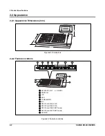
Page 8: ...ns mm 155 2 4 2 378 Figure2 1 Dimensions 2 2 2 Feature Locations 1 2 3 4 7 8 6 5 9 10 11 Figure2 2 Feature Locations KEYBOARD FLAT or RAISED MODE KEY LCD MCR POWER SMPS IRC RS232 Serial I F 4 RJ45 RS2...

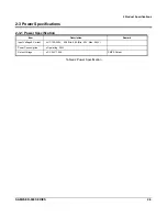
Page 9: ...2 3 2 3 Power Specifications 2 3 1 Power Specification Item Description Remark Input Voltage Current AC 100 240V 50 60Hz 0 8A Min 90V Max 264V Power Consumption Operating 25W Output Voltage DC 24V 1...

Page 10: ...Logic 0 SPACE 3V 15V Baud Rate 1200 2400 4800 9600 19200 bps Data Word Length 7 Bit 8 Bit Parity None Even Odd Connector DB9P Female RS 232 1 2 RJ 45 3 4 Voltage Supply VCC 5V 200mA is supplied at 9P...

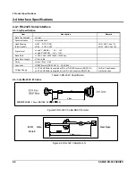
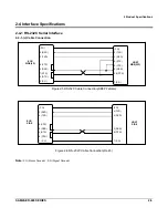
Page 11: ...2 5 RS232C Cable Connection DB9P Female Figure 2 6 RS 232C Cable Connection RJ 45 Note F G Frame Ground S G Signal Ground F G 2 RXD 3 TXD 8 CTS 6 DSR 7 RTS 4 DTR 5 S G F G 2 TXD 3 RXD 4 RTS 5 CTS 6 DS...

Page 12: ...0mA is total value including COM1 and COM4 Power Consumption If the Total Power Consumption of the attached devices is exceeded the specification 200mA the system stops the VCC of D SUB Connector Caut...

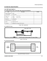
Page 13: ...d Rate 9600 bps Only Data Word Length 7 Bit 8 Bit Parity None Even Odd Connector Modular Jack Connector 12P 2Port 6Pin Table2 5 IRC Specification 2 4 2 b IRC I F Cable Figure2 7 IRC Cable 2 4 2 c Cabl...

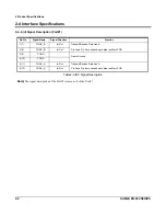
Page 14: ...X_B In Out 2 8 TX RX_B In Out Transmit Receive Data Line B Pin 1 and Pin 2 are shorted each other on Main PCB 3 9 F GND 4 10 F GND Frame Ground 5 11 TX RX_A In Out 6 12 TX RX_A In Out Transmit Receive...

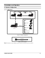
Page 15: ...3 Installation and Operation 3 1 System Configuration 3 1 1 Configuration Figure 3 1 System Configuration Figure 3 2 IRC Terminator Note The termination resistor 120 Ohm must be installed at Host ECR...

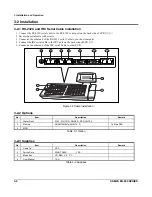
Page 16: ...st computer 4 Connect the IRC serial cable to the IRC port on the back side of ECR 5 Connector the other end of the IRC serial Cable to other ECR 1 2 3 4 7 8 6 5 9 10 11 Figure 3 3Cable Installation 3...

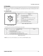
Page 17: ...normal registrations X Use to read register reports and perform other manager functions Z Use to read register reports and reset totals to zero PGM Use to program the register SM Use for H W tests and...

Page 18: ...WARNING This is a one time procedure Do not repeat this procedure after the cash register is programmed it causes all programs and totals to be erased and to be default 1 Turn off the power switch 2...

Page 19: ...ile and PORT 8 Select the Boot area only 9 Click OK 3 3 5 Program Area Download 1 Turn off the power switch 2 Connect the serial 1 cable of register to PC 3 Turn the mode switch to SM MODE 4 Press and...

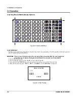
Page 20: ...will be showed on the LCD 5 Turn the mode key to any position to finish this test 3 3 6 d Test Mode Key 1 Turn on the power switch 2 Press Press 0 and 3 key on key board 3 Turn the mode key to any po...

Page 21: ...T MCR A 8 from the MCR CARD READER A 7 When the ASS Y CASE UPPER A doesn t have the MCR CARD READER A 7 first follow the 1 2 and 3 like above and then Separated the COVER MCR A 1 from the CASE UPPER A...

Page 22: ...Y CASE UPPER D ASS Y KBD RAISED E ASS Y KBD FLAT C ASS Y CASE LOWER B ASS Y DISPLAY A 1 A 3 A 4 A 5 A 6 A 7 A 8 A 9 A 10 C 13 C 14 C 10 C 11 C 15 C 16 C 17 C 18 C 19 C 12 A 2 B 1 C 1 C 4 C 2 C 3 C 5 C...

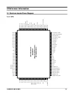
Page 23: ...P8 3 INT1 P8 4 INT2 P8 5 NMI VCC XIN VSS XOUT RESET P8 6 XCOUT P8 7 XCIN CNVSS BYTE P9 0 TB0IN CLK3 P9 1 TB1IN RXD3 SCL3 P9 2 TB2IN TXD3 SDA3 P9 3 DA0 TB3IN CTS3 P9 4 DA1 TB4IN CTS4 P9 5 ANEX0 CLK4 P9...

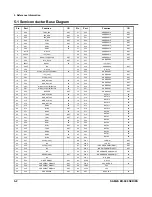
Page 24: ...P2 1 ADDRESS1 OUT 22 P8 0 BUZZER OUT 72 P2 0 ADDRESS0 OUT 23 P7 7 MCR_CLS2 3 IN 73 P1 7 DATA15 I O 24 P7 6 MCR_RDT2 3 IN 74 P1 6 DATA14 I O 25 P7 5 MCR_CLS1 2 IN 75 P1 5 DATA13 I O 26 P7 4 MCR_RDT1 2...

Page 25: ...5 6 7 8 9 10 11 12 13 14 15 16 32 TSOP2 A16 A14 A12 A7 A6 A5 A4 A3 A2 A1 A0 I O1 I O2 I O3 VSS VCC A15 WE A13 A8 A9 A11 OE A10 CS I O8 I O7 I O6 I O5 I O4 32 31 30 29 28 27 26 25 24 23 22 21 20 19 18...

Page 26: ...1 10 9 8 2 1 3 4 5 6 7 VCC B4 A4 Y4 B3 A3 Y3 A1 B1 Y1 A2 B2 Y2 GND Inputs Outputs CS1CS2 CS3 A2 A1 A0 Y0 Y1 Y2 Y3 Y4 Y5 Y6 Y7 X X H X X X H H H H H H H H X H X X X X H H H H H H H H L X X X X X H H H...

Page 27: ...smitted from Bus A to Bus B H X Buses Isolated High Impedance State X don t care 18 Y1 2 A1 17 Y2 3 A2 16 Y3 4 A3 15 Y4 5 A4 14 Y5 6 A5 13 Y6 7 A6 12 Y7 8 A7 11 Y8 9 A8 OE1 OE2 1 19 Output Enables Dat...

Page 28: ...to select input frequency range and output frequency scaling Refer to Tables 7 8 for selection S0 has internal pulldown S1 has internal pullup 4 LF I Analog Loop Filter Single ended tri state output o...

Page 29: ...A34063 Figure 5 14 M51953 INTRB 1 VDD 5 SCL 2 OSCIN 6 SDA 3 OSCOUT 7 VSS 4 INTRA 8 Figure 5 15 RS5C372A 1 Switch Collector Switch Emitter Timing Capacitor Gnd Driver Collector I pk Sense VCC Comparato...

Page 30: ...ransistor Diode KSA1010 Y KSD288 Y KSA708 Y KSA1182 Y MMBT2222A MMBD6050 1 Base 2 Collector 3 Emitter 1 TO 220 1 Emitter 2 Base 3 Collector TO 92 1 SOT 23 1 2 3 1 Base 2 Emitter 3 Collector SOT 23 1 2...

Page 31: ...ge sources and one AC voltage source Figure 6 1 Power Block Diagram No Voltage Description 1 VDRV 24VDC Cash Drawer Solenoid Driving 2 VCC 5VDC Logic IC Driving VFD Filament Voltage 3 VBT Min 3 6VDC B...

Page 32: ...driving voltage is produced by the step down dc dc converter U26 34063A That is U26 produces rectangular wave at the collector of Q14 A1010 by switching Q14 using 24VDC This makes D28 IN5822 and L40 s...

Page 33: ...ects sudden power off to backup the needed data and current CPU status into RAM before 80ms just before 5V drops When power is turned on the CPU does the operations which were working before power off...

Page 34: ...R34 270 VBT BAT1 22uF C31 50V D17 DIODE M4 DIODE SK14 D14 Figure 6 3 Battery Circuit 6 3 2 RTC Clock Circuit This uses an Clock IC RS5C372 is driven by the Battery when the main Power is turned off V9...

Page 35: ...cash drawer As an optional item we provide sensor switch we call it a compulsory switch which checks the drawer whether it is opened or not This sensor switch turns on for the drawer open condition an...

Page 36: ...Modular 6P SERIAL 1 2 MAX232 DRIVER MAX232 DRIVER IRC DRIVER SERIAL 3 4 TXD1 RXD1 DTR1 DSR1 TXD2 RXD2 DTR2 DSR2 T RXD T RXD TRANSMIT ACTION ECR RECEIVE ACTION ECR HOST BUSY ECR checks whether the host...

Page 37: ...munication Block Diagram Figure 6 9 IRC Waveform TRANSMIT ACTION ECR RECEIVE ACTION ECR H Transmission a data 1 Byte DATA TX RX_A TX RX_B L Level Gnd Level Gnd Level 5V Level 5V Received data 1 Byte T...

Page 38: ...during the given time The CPU reads the data through U7 74HC541 and analyzes what key is pressed and transmits this information to the CPU then performs the selected function The Key Board Circuit sen...

Page 39: ...the Power Cable 2 Replace the SMPS Power VDRV 24V Ok 1 Check the Fuse FU1 on PCB 2 Check the Diode D36 D37 ZD 6 on PCB 3 Check the VDRV signal whether it is short N Power VCC 5V Ok Y Y 1 Check the IC...

Page 40: ...through RS 232 Cable 4 Replace the Flash ROM 1 Check the LM393 U15 2 Check the Power 24V 5V 3 Check the related Circuit and Pattern on PCB N N SRAM Ok Y Y N CPU Ok Y N 1 Check the nCS nRD nWR signal...

Page 41: ...Scan Part 74HC138 U1 U24 3 Check the Key Return Part 74HCT541 4 Check the related Circuit and Pattern 5 Check Change Key Board Assy 6 Check the KBD Connector on PBA Specific Key Failure 1 Check the a...

Page 42: ...ack Failure Y N 1 Perform the SELF TEST in the SM MODE using the Loop Back test Connector 2 Check the connection of the RS 232C Connector and Loop Back Connector 3 Check the TXD RXD Pin on CPU 4 Check...

Page 43: ...View A ASS Y CASE UPPER D ASS Y KBD RAISED E ASS Y KBD FLAT C ASS Y CASE LOWER B ASS Y DISPLAY A 1 A 3 A 4 A 5 A 6 A 7 A 8 A 9 A 10 C 13 C 14 C 10 C 11 C 15 C 16 C 17 C 18 C 19 C 12 A 2 B 1 C 1 C 4 C...

Page 44: ...G PH 2 M3 L10 ZPC YEL 2 Y B 7 JK97 20004A PMO COVER REAR LCD HIPS VO 1 Y B 8 JK72 20044A PMO CAP HIPS VO 1 Y 8 1 2 c ASS Y CASE LOWER No Parts No Description Specification Q ty Design Location Service...

Page 45: ...ENT ER 600R STD 1 Y JK59 30008C UNIT KEYBOARD NUMERICAL ER 600R EUROPE 1 Y JK59 30008D UNIT KEYBOARD NUMERICAL ER 600R ENGLAND 1 Y JK59 30008E UNIT KEYBOARD NUMERICAL ER 600R SPAIN 1 Y D JK59 30008F U...

Page 46: ...TOP 1 1 Y JK81 10934A KEY TOP 2 1 Y JK81 10935A KEY TOP 3 1 Y JK81 10936A KEY TOP 4 1 Y JK81 10937A KEY TOP 5 1 Y JK81 10938A KEY TOP 6 1 Y JK81 10939A KEY TOP 7 1 Y JK81 10940A KEY TOP 8 1 Y JK81 109...

Page 47: ...F 1 Y JK68 40009A LABEL P KEYBOARD NUMERICAL ER 600F USA 1 Y JK68 40009B LABEL P KEYBOARD NUMERICAL ER 600F EUROPE 1 Y JK68 40009C LABEL P KEYBOARD NUMERICAL ER 600F ENGLAND 1 Y JK68 40009D LABEL P KE...

Page 48: ...8 Exploded Views and Parts List 8 6 SAM4S ER 600 SERIES MEMO...

Page 49: ...SAM4S ER 600 SERIES 9 1 9 PCB Layout and Parts List 9 1 Main PCB Layout 9 1 Component Side View PCB JK41 10549A...

Page 50: ...3 U5 Y 3711 001133 CONNECTOR HEADER BOX 8P 1R 2 5mm STRAIGH 2 CN1 CN13 Y 3711 000190 CONNECTOR HEADER 1WALL 2P 1R 7 92mm STRA 1 CN15 Y 3711 001475 CONNECTOR HEADER NOWALL 3P 1R 2 54mm STR 1 CN10 Y 371...

Page 51: ...D4 D10 D17 D26 Y 0401 001003 DIODE SWITCHING MMBD6050LT1 70V 200mA 22 5 D1 D2 D3 D5 D6 Y 0401 001003 DIODE SWITCHING MMBD6050LT1 70V 200mA 22 5 D7 D8 D9 D11 D12 Y 0401 001003 DIODE SWITCHING MMBD6050...

Page 52: ...P 3 3KOHM 5 1 10W DA TP 2012 2 R39 R64 Y 2007 001662 R CHIP 36KOHM 1 1 10W DA TP 2012 1 R86 Y 2007 000941 R CHIP 47KOHM 5 1 10W DA TP 2012 1 R79 Y 2007 000352 R CHIP 12KOHM 1 1 10W DA TP 2012 1 R91 Y...

Page 53: ...2nF 10 50V X7R TP 2012 2 C78 C80 Y 2203 000595 C CERAMIC CHIP 0 22nF 5 50V NP0 TP 2012 1 C86 Y 2203 000239 C CERAMIC CHIP 0 1nF 5 50V NP0 TP 2012 2 C91 C92 Y 0202 000108 SOLDER CREAM RMA 010 T 322 S6...

Page 54: ...9 PCB Layout and Parts List 9 6 SAM4S ER 600 SERIES MEMO...

Page 55: ...SAM4S ER 600 SERIES 10 1 10 Block Diagram 10 1 ER 600...

Page 56: ...10 Block Diagram 10 2 SAM4S ER 600 SERIES MEMO...

Page 57: ...EN_DWRCOMP2_IN 9 GND 9 VSERIAL 10 D3 10 VDRV 10 GND 10 FGND 11 D4 11 DRAWER2_OUT 11 TPTX 11 FGND 12 D5 12 GND 12 TPTX 13 D6 14 D7 CN13 MCR CN7 RS232 CN8 RS232 15 CE1 NO SIGNAL NAME NO SIGNAL NAME NO S...

Page 58: ...11 Wiring Diagram 11 2 SAM4S ER 600 SERIES 11 2 Wiring Diagram Figure11 1 Wiring Diagram...

Page 59: ...tic Diagrams Schematics Sheet Content 1 Main PCB Schematics 1 CPU Block 12 2 2 Memory RTC Decoder Block 12 3 3 Power Control Block 12 4 4 Serial I F Block 12 5 5 Key Mode S an Block 12 6 6 Display LCD...

Page 60: ...TXD4_IRC RXD4_IRC IRC_DEN IRC_REN V133 V136 MEM_CE P8 6 Mode Key Scan Common Signal RTC_SCLK V121 MCR_RCL2 3 MCR_RCL1 2 V111 V155 BUZZER INT0_PFAIL Buzzer Note Use Timer_A4 Block MCR_CLS2 3 MCR_RDT2 3...

Page 61: ...80000 0X2FFFFF 4MBits 0x200000 0X27FFFF 4MBits R29 100 R25 100 R22 100 R21 100 CS_RAM4M1 CS_RAM4M2 A 2 A 5 A 8 A 2 A 5 A 8 VBT VBT A 17 A 11 A 14 A 17 A 11 A 14 CPU SYSTEM PART R33 100 CS_RAM4M3 CS_RA...

Page 62: ...VCC VDRV 2 3 1 MMBT2222A Q7 VCC R19 100 VCC D20 V1 2 R65 4 7K 2 3 1 MMBT2222A Q9 R67 10K BAT1 15K R37 3 3K R39 R2 10K R1 10K R40 4 7K C41 100nF D4 DIODE M4 2 2K R47 R24 10K R42 4 7K R20 100 D21 CS_EXT...

Page 63: ...CN10 A CON NOWALL 3P 2 54MM ST 7 CN7 G L30 4 CN7 D 5 CN6 E 1 CN6 A L25 2 CN6 B IRC_DEN TXD4_IRC 11 CN5 K RXD4_IRC IRC_REN 5 CN5 E 8 CN5 H 1 CN5 A L23 4 CN5 D L21 2 CN5 B L22 3 CN5 C ER 600 EASYCASH MA...

Page 64: ...1 4 7 CN1 7 6 CN1 6 Yun Choi V1 2 D29 D30 D12 VCC VCC VCC A 3 CS_KBDMODE V190 V181 V183 A 2 A 1 V175 V177 A 0 V170 V171 V166 A 4 CS_KBDMODE A 2 A 0 8 CN11 H 6 CN11 F 4 CN11 D 2 CN11 B CS_KBDMODE 7 CN3...

Page 65: ...7K R72 R90 4 7K R99 4 7K 2 3 1 MMBT2222A Q11 470 R73 V185 V180 V188 V174 VCC V167 V158 C90 100nF C81 100nF C85 100uF 16V SIG NAME CE3 192 64 19 16 15 14 13 10 8 9 7 20 21 22 4 2 3 D5 EN nRESET SIG NAM...

Page 66: ...ND N C VDRV C88 100nF R96 0 1 L49 C86 220pF 1N4003 D36 FU1 FUSE 1N4751A ZD6 C89 100nF VDRV C68 100nF C79 470uF 16V 12K R91 2003 06 28 Yun Choi V1 2 L50 R87 560 1 4W 3 2 1 Q14 KSA1010Y D28 1N5822 R86 3...

Page 67: ...page to record any special servicing information such as Service Bulletins or Supplements When possible record changes to Code numbers directly on the actual Parts List Always record Service Bulletin...

Page 68: ...Shin Heung Precision FEBRUARY 2004 Printed in KOREA V1 1 Code No JK68 60935A...

Reviews: