UPS25 28
RTD Embedded Technologies, Inc
Chapter 5
- B
OARD OPERATION AND PROGRAMMING
This chapter shows you how to program and use your UPS25. It provides a
complete detailed description of the I/O map and a detailed discussion of
programming operations to aid you in programming.
Defining the Memory Map
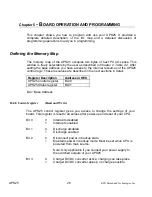
The memory map of the UPS25 occupies two bytes of host PC I/O space. This
window is freely selectable by the user as described in Chapter 2, Table 2-2. After
setting the base address you have access to the internal resources of the UPS25
control logic. These resources are described in the next sections in detail.
Register Description
Address in HEX
UPS25 Control register
BA+0
UPS25 Status register
BA+1
BA = Base Address
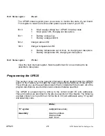
BA+0 Control register
(Read and Write)
The UPS25 control register gives you access to change the settings of your
board. This register is reset to all zeroes after power-up and reset of your CPU.
Bit 0
0
Interrupts disabled
1
Interrupts
enabled
Bit 1
0
Discharge disabled
1
Discharge
enabled
Bit 2
0
Disconnect power in backup state
1
Maintains power in backup mode. Must be set while CPU is
powered from main source.
Note: Only applicable if you connect your power supply to
the switched outputs of your UPS25.
Bit 3
0
Charger DC/DC converter active, charging can take place
1
Charger DC/DC converter asleep, no charge possible


