background image

12

DS8241-03   January  2014

www.richtek.com

RT8241

©

Copyright   2014 Richtek Technology Corporation. All rights reserved.                          is a registered trademark of Richtek Technology Corporation.

If the V

OUT

 change is significant, there can be several

consecutive cycle of UGATE on-time followed by minimum

LGATE time. This can cause a rapid increase in inductor

current: typically it only takes a few switching cycles for

inductor current to rise up to the current limit. At some

point the V

FB

 will rise up to the new internal V

REF

 and the

UGATE pulses will cease, but the inductor's LI

2

 energy

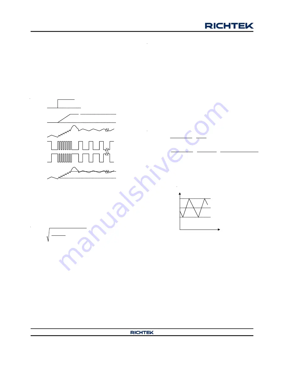
must then flow into the output capacitor. This can create

a significant overshoot, as shown in Figure 5.

Figure 5. Output Voltage Up Transition with

Overshooting

This overshoot can be approximated by the following

equation, where I

CL

 is the current limit, V

FINAL

 is the

desired set point for the final voltage, L is in 

μ

H and C

OUT

is in 

μ

F.

2

2

CL

MAX

FINAL

OUT

I

L

V

(

) V

C

×

=

+

Current Limit Setting (OCP)

The RT8241 has a cycle-by-cycle current limiting control.

The current limit circuit employs a unique 

valley

 current

sensing algorithm. If the magnitude of the current sense

signal at the CS pin is above the current limit threshold,

the PWM is not allowed to initiate a new cycle (Figure.

6). In order to provide both good accuracy and a cost

effective solution, the RT8241 supports temperature

compensated MOSFET R

DS(ON)


sensing. The CS pin

should be connected to GND through the trip voltage setting

resistor, R

CS

. The 10

μ

A CS terminal source current , I

CS

,

and the trip voltage setting resistor, R

CS

, set the CS trip

CS

CS

V

(mV)  =  R

(k ) 10( A)

μ

Ω ×

The Inductor current can be monitored by the voltage

between GND and the PHASE pin. Hence, the PHASE

pin should be connected to the drain terminal of the low

side MOSFET. I

CS

 has temperature coefficient to

compensate the temperature dependency of the R

DS(ON)

.

GND is used as the positive current sensing node, so

GND should be connected to the source terminal of the

bottom MOSFET.

While the comparison is being done during the OFF state,

V

CS

 sets the valley level of the inductor current. Thus, the

load current at over-current threshold, I

LOAD_OC

, can be

calculated as follows :

ripple

CS

LOAD_OC

DS(ON)

CS

IN

OUT

OUT

DS(ON)

SW

IN

I

V

I

8 R

2

V

(V

V

) V

1


8 R

2 L f

V

=

+

×

×

=

+

×

×

× ×

In an over-current condition, the current to the load exceeds

the current to the output capacitor, thus causing the output

voltage to fall. Eventually the voltage crosses the under

voltage protection threshold and the device shuts down.

Figure 6. “ Vally”  Current Limit

Negative Over Current Limit (PWM Only Mode)

The RT8241 supports cycle-by-cycle negative over current

limiting in CCM Mode only. The over current limit is set to

be negative but is the same absolute value as the positive

over current limit. If output voltage continues to rise, the

low side MOSEFT remains on. Thus, the inductor current

is reduced and reverses direction after it reaches zero.

When there is too much negative current in the inductor,

the low side MOSFET is turned off and the current flows

towards V

IN

 through the body diode of the high side

MOSFET. Because this protection limits the discharge

current of the output capacitor, the output voltage tends

0

I

L

t

I

L_Peak

I

LOAD

I

LIM

voltage, V

CS

, as in the following equation.

GND

Gx

V

REF

Initial V

REF

Final V

REF

V

FB

UGATE

LGATE

Initial V

OUT

Final V

OUT

V

OUT

Summary of Contents for RT8241

Page 1: ...n high voltage batteries at the highest possible efficiency The RT8241 is intended for CPU core chipset DRAM or other low voltage supplies as low as 0 675V The RT8241 is available in a WQFN 12L 2x2 pa...

Page 2: ...LOUT 8 G1 VIN CIN VOUT COUT Optional R2 Chip Enable VCC RT8241 VCC 5 9 6 PGOOD EN 11 CS 12 13 Exposed Pad GND 4 BOOT 3 2 1 7 10 UGATE PHASE LGATE G0 FB R1 CBYPASS RCS R3 C1 R4 Q1 Q2 R5 C2 LOUT 8 G1 VI...

Page 3: ...d the bootstrap circuit for high side driver Bypass to GND with a 4 7 F ceramic capacitor 6 EN Chip Enable Active High 7 G0 2 Bit Input Pin 8 G1 2 Bit Input Pin 9 PGOOD Open Drain Power Good Indicator...

Page 4: ...C to 150 C z ESD Susceptibility Note 3 HBM Human Body Mode 2kV MM Machine Mode 200V Recommended Operating Conditions Note 4 z Supply Input Voltage VIN 4 5V to 26V z Control Voltage VCC 4 5V to 5 5V z...

Page 5: ...er Voltage Lockout UVLO Threshold VUVLO Falling edge PWM disabled below this level 3 5 3 7 3 9 V VCC UVLO Hysteresis VUVLO 100 mV VOUT Soft Start From EN High to VOUT 95 0 8 ms Dynamic VID Slew Rate S...

Page 6: ...1 A Note 1 Stresses listed as the above Absolute Maximum Ratings may cause permanent damage to the device These are for stress ratings Functional operation of the device at these or any other conditi...

Page 7: ...Frequency kHz 1 VIN 8V VCC VEN 5V VOUT 0 9V Efficiency vs Output Current 60 65 70 75 80 85 90 95 100 0 001 0 01 0 1 1 10 Output Current A Efficiency VIN 12V VCC VEN 5V VOUT 0 9V Switching Frequency vs...

Page 8: ...V VCC VEN 5V VOUT 0 8V to 0 9V VOUT 50mV Div 0 9V Shutdown Current vs Input Voltage 0 0 0 1 0 2 0 3 0 4 0 5 0 6 0 7 0 8 0 9 1 0 5 7 9 11 13 15 17 19 21 23 25 Input Voltage V Shutdown Current A 1 NoLoa...

Page 9: ...ransient Response Time 100 s Div VIN 12V VCC VEN 5V VOUT 0 9V ILOAD 0A to 6A ILOAD 5A Div VOUT_ac 20mV Div LGATE 10V Div UGATE 20V Div Over Voltage Protection PGOOD 5V Div VOUT 500mV Div LGATE 5V Div...

Page 10: ...this capacitor to charge from zero volts to VOUT thereby making the on time of the high side switch directly proportional to the output voltage and inversely proportional to the input voltage The imp...

Page 11: ...trigger NOCP the low side MOSFET will be turned off to prevent Figure 3 Output Voltage Down Transition LGATE PHASE UGATE FB G0 G1 G0 G1 Q1 Q2 CIN VIN RFB1 RFB2 BOOT VOUT COUT For an upward transition...

Page 12: ...e CS trip CS CS V mV R k 10 A The Inductor current can be monitored by the voltage between GND and the PHASE pin Hence the PHASE pin should be connected to the drain terminal of the low side MOSFET IC...

Page 13: ...e MOSFET without degrading the turn off time as shown in Figure 7 Figure 7 Reducing the UGATE Rise Time PHASE UGATE Q1 CIN VIN BOOT R Power Good Output PGOOD The power good output is an open drain out...

Page 14: ...nd cause erratic and unstable operation However it is easy to add sufficient series resistance by placing the capacitors a couple of inches downstream from the inductor and connecting FB divider close...

Page 15: ...ines should be strictly followed Connect an RC low pass filter from VCC 1 F and 10 are recommended Place the filter capacitor close to the IC Keep current limit setting network as close as possible to...

Page 16: ...ccurate and reliable However no responsibility is assumed by Richtek or its subsidiaries for its use nor for any infringements of patents or other rights of third parties which may result from its use...

Reviews: