SERVICE , MANUAL
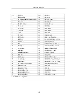
34
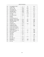
Output terminal for AV2 on/off control
5.30
11.8
6.36
35
Output terminal for AV1 on/off control
5.30
11.4
6.33
36
Output terminal for AV0 on/off control
5.29
141.2
6.33
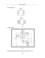
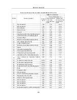
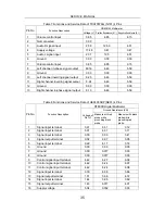
Table 4 Functions and Service Data of AT24C04/ST24C04 (D702)’s Pins
DT890D Digital Multimeter
Ground Resistance ( )Negative Resistance(k )
Pin No.
Function Description
Voltage of
Pin (V)
Measure with red
probe while
grounding black
probe.
Measure with black
probe while
grounding red
probe.
1
Address input terminal
0.00
0.00
0.00
2
Address input terminal
0.00
0.00
0.00
3
Address input terminal
0.00
0.00
0.00
4
Common ground
0.00
0.00
0.00
5
Clock line
4.94
6.85
4.83
6
Data line
4.94
6.89
5.15
7
PW write protection terminal
0.00
9.58
5.31
8
Supply voltage
5.32
3.5
3.25
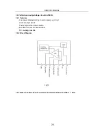
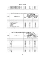
Table 5 Functions and Service Data of KA2102B/K2192B (NV01)’s Pins
DT890D Digital Multimeter
Ground Resistance (K )
Pin No.
Function Description
Voltage of
Pin (V)
Measure with red
probe while
grounding black
probe.
Measure with
black probe while
grounding red
probe.
1
L TV IN
5.67
6.45
3.53
2
R TV IN
5.67
6.45
3.74
3
TV IN
5.67
6.57
4.02
4
LS IN
5.69
6.45
3.66
5
RS IN
5.69
6.47
3.72
6
SY IN
5.54
6.85
3.96
7
TV SW
0.00
0.00
0.00
8
SC IN
5.54
6.75
3.85
9
L1 IN
5.69
6.43
3.36
10
R1 IN
5.70
6.37
3.72
11
E1 IN
5.56
6.85
3.96
12
L2 IN
5.70
6.43
3.87
33
Summary of Contents for MCR51R410
Page 15: ...14 STRUCTURE AND CHASSIS FUNCTION DESCRIPTION 1 Structure Block Diagram ...
Page 16: ...15 2 Block Diagram for Supply Voltage System ...
Page 17: ...16 3 System Control Block Diagram ...
Page 38: ......
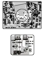
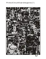
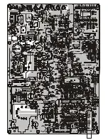
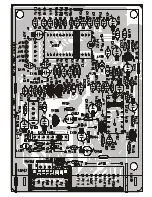
Page 39: ...Printed Circuit Board diagrams 1 ...
Page 40: ......
Page 41: ......

