background image

RANDOM*SOURCE


RANDOMSOURCE.NET

3

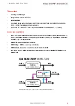
J. HAIBLE Dual WASP Filter (Euro)

The R*S kit consists of a main pcb and a matching panel pcb which serves as an interface to the front panel. 
Bot pcbs version 1.00 are through-hole (TH) with only very few optional SMT parts (BCM857 on the main pcb 
and dual op-amp on the panel pcb):

Please note:


• 

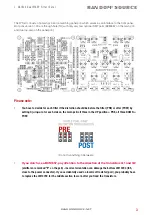
You have to decide for each filter if the distortion should be before the filter (PRE) or after (POST) by 
setting 

3 jumpers

 for each side on the main pcb: all three in the UP position = PRE, all three DOWN = 

POST:  

(Do not try anything in between!)

• 

If you don’t use a BCM857, pay attention to the direction of the transistors Q1 and Q2


(emitters are marked “E” on the pcb) - incorrect orientation can damage the bottom LM13700 (IC5, 
close to the power connector). If you accidentally used an incorrect trasistor (pair), you probably have 
to replace the LM13700 for the middle section to work after you fixed the transistors.

Summary of Contents for JHAIBLE Dual WASP Filter

Page 1: ...in there too creating infinite filterbank combinations A Sync switch has been added to be able to control both side s cutoff frequency with from the left side The unique distortion can be configured t...

Page 2: ...t side too This opens up amazing possibilites use both sides separately turn MODE to parallel as a stereo filter or set MODE to serial for a 4 pole 24db WASP filter MODE knob blend from SERIAL to PARA...

Page 3: ...the distortion should be before the filter PRE or after POST by setting 3 jumpers for each side on the main pcb all three in the UP position PRE all three DOWN POST Do not try anything in between If...

Page 4: ...and a link from pin 1 to 2 center or 3 Be careful 2 of the op amps left and right are SINGLE The ones in the center row are DUAL Do not confuse SINGLE and DUAL op amps up or they will burn There s a d...

Page 5: ...R57 R62 11 1k R25 AR1 AR2 R5 R9 R25B R26A R26B R32 R36 R77 2 1k AR3 AR4 Taper for Cutoff Pot 2 1k5 R24B R24 7 4k7 R19 R20 R46 R47 R59 R64 R69 2 5k1 R27 R27B sets CV range 7 10k R75 AD7 AD14 R72 R73 R...

Page 6: ...IC10 SMT Dual Op amp eg OPA2134 TL072 SOIC8 2 BC560 Q1 Q2 PNP Transistor BC560C Alternative to BCM857 Do not install both 1 BCM857DS Q1A NXP BCM857 SMT instead of Q1 Q2 Potentiometers Alpha 9mm vertic...

Page 7: ...t matching the pin headers to connect to the panel pcb this gets more difficult once the component pcb is connected to the front panel and insert the pin headers connecting the pcbs Main pcb and panel...

Page 8: ...alled TRIM X and TRIM Y simply feed a audio signal ideally a pulse wave around 1kHz or so into the CV Mode input set the MODE knob to CCW minimum and turn the CV Mode knob all the way up make sure the...

Page 9: ...scope using the test pads x TP IN y on y you see the signal going into the VCA on x the output of the first VCA If you have a signal on IN y but not on x swap the lower LM13700 near the power connect...

Reviews: