RANDOM*SOURCE
RANDOMSOURCE.NET
7
J. HAIBLE Dual WASP Filter (Euro)
Power Connector
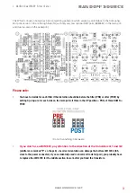
The module is designed to be powered using a standard Eurorack 10-pin DIP header (12V / GND /
GND / GND / -12V with the
red stripe on the cable indicating the -12V side
).
Builing choices
Trimmers
: Trimming concerns only the MODE (mix) circuitry and does not seem essential. CV rejection (TRIM X
and TRIM Y) can easily done by ear (see calibration info below), while the BIAS trimming requires a good scope,
so installing the BIAS trimmers makes no sense unless you’re sure that you want to do the calibration (which is
easy with a scope).
Op-amps
: the OPA2134 and OPA134 are hard to beat in performance, however, feel free to experiment with
other choices, just make sure you
don’t mix up single and dual
.
Building
1.
Use a side-cutter to separate main pcb and component pcb.
2.
Main pcb and component pcb are to be connected through precision SIP sockets and pins (pin
headers). It is recommended to use the pins on the main pcb (facing down, soldered from above)
and the pin sockets on the component pcb (standing up, soldered from the front panel side).
Break or cut off the pieces you need and stick them together.
3.
Attach screws / spacers (10mm or hight matching the pin headers to connect ) to the panel pcb
(this gets more difficult once the component pcb is connected to the front panel) and insert the
pin headers connecting the pcbs. Main pcb and panel pcb should form a nice sandwich (don‘t sol-
der yet). Check that you didn‘t leave out any pins / holes and that the sockets are all on the same
side (component pcb). Solder all the pins in while keeping the sandwich together - this avoids any
misalignments.
4.
Carefully
separate the sandwich - if you used precision sockets, this may not to too easy - they
stick together nicely (giving a good connection).
5.
Mount the Thonkiconn jacks, the pots and the switches onto the panel pcb. Pots should sit on the
side facing the front panel (as marked on the board). Don‘t solder them in yet.
6.
Either solder the SMT op-amp (OPA2134 or TL072 in SOIC8) onto the panel pcb
or
install links /
zero ohm (0R) resistors in the spots marked RLX - not both!
7.
Insert and solder the BP (Audio) Caps (C10, C11) and the LED trimmers (or resistors - not both!)
onto the panel pcb. The BP caps should lie (flat) between the Thonkiconn jacks.
8.
Carefully mount the panel pcb (with the pots etc. inserted) onto the front panel. You may then
have to wiggle each pot a bit to get the pots through. Make sure the threads of the pots go
through completely and the pots sit right at the front panel. Screw the jacks, pots and switches to
the the front panel to make sure of that.


