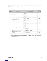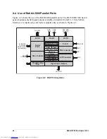
background image

Getting Started Manual

29

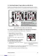
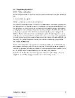
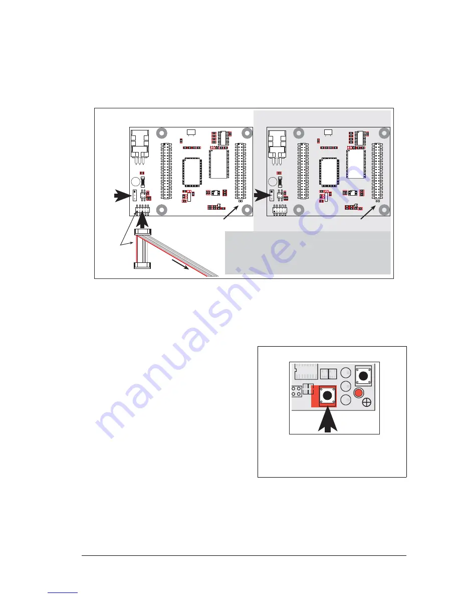
3.3  Switching Between Program Mode and Run Mode

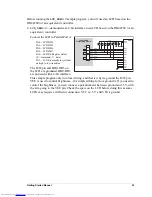
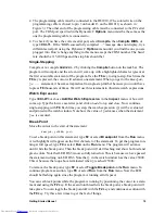
The BL1810 is automatically in Program Mode when the programming cable is attached, 
and is automatically in Run Mode when no programming cable is attached. See Figure 5.

Figure 5.  BL1810 Program Mode and Run Mode Setup

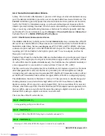
3.3.1  Detailed Instructions: Changing from Program Mode to Run Mode

1. Disconnect the programming cable from header J3 of the BL1810.

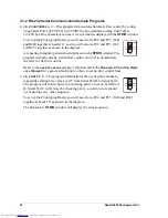
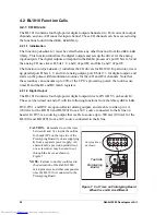
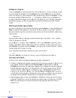
2. Reset the BL1810. You may do this as explained in Figure 5. Figure 6 shows the loca-

tion of the RESET button on the Prototyping Board.

The BL1810 is now ready to operate in the Program Mode. 

2. Reset the BL1810. You may do this as 

explained in Figure 5. Figure 6 shows the 
location of the RESET button on the Proto-
typing Board.

The BL1810 is now ready to operate in the Run 
Mode. 

3.3.2  Detailed Instructions: Changing 
from Run Mode to Program Mode

1. Attach the programming cable to header J3 

on the BL1810.

Figure 6.  Location of Prototyping Board 

Reset Button

JP1

Program Mode

JP1

Run Mode

Power

RESET BL1810 when changing mode:

 Short out 

RESET

 pads below header J5, 

OR

 Press 

RESET

 button (if using Prototyping Board), 

OR

 Remove, then reapply power

after removing or attaching programming cable.

Reset pads

Reset pads

U4

U4

VIN
GND

GND

RESET

JACKRABBIT Z-World, Inc.

GND

PA0
PA2
PA4
PA6

GND

PB0
PB2
PB4
PB6

WDO

GND

PE6
PE4
PE2
PE0
HV0
HV2

K

GND

VCC
PA1
PA3
PA5
PA7
GND
PB1
PB3
PB5
PB7
PCLK
PE7
PE5
PE3
PE1
GND
HV1
HV3
+RAW
VCC

GND
RXC
TXC
PC1
PC3
PC5
PC7
AGND
DA1
PD1
PD3
PD5
PD7
GND
485+
VCC
SM1
STAT
VBAT
GND

VCC
RXB

TXB
PC0
PC2
PC4
PC6
AD0
DA0
PD0
PD2
PD4
PD6

GND
485–

VCC
SM0

IOBEN

GND
/RST

J5

U6

U5

U3

J4

U1

J1

J2

J3

Y3

Rabbit 2000

SRAM

RS-232

RS-485

Colored side

lines up with

pin 1

To

PC 

COM

 port

PROG

DIAG

Programming

connector

J6

S4

DS9

DS6

DS7

DS8

S5

/RST

GND

IOBEN

S

TAT

VBA

T

RESET

PWR

GND

Downloaded from 

Elcodis.com


electronic components distributor


Summary of Contents for 2000

Page 1: ...Rabbit 2000 Microprocessor Development Kit Getting Started Manual 019 0068 050515 F Downloaded from Elcodis com electronic components distributor...

Page 2: ...umber 019 0068 050515 F Printed in U S A 2000 2005 Z World Inc All rights reserved Z World reserves the right to make changes and improvements to its products without providing notice Trademarks Rabbi...

Page 3: ...14 2 5 Run a Sample Program 14 2 5 1 Troubleshooting 14 2 6 Where Do I Go From Here 15 2 6 1 Technical Support 15 Chapter 3 Sample Programs 17 3 1 Running Sample Program DEMOJR1 C 18 3 1 1 Other Samp...

Page 4: ...rmation 39 A 1 Electrical and Mechanical Specifications 40 A 2 Header Pinout 41 A 3 Jumper Configurations 42 A 4 Use of Rabbit 2000 Parallel Ports 44 Notice to Users 45 Index 47 Schematics 49 Download...

Page 5: ...bit 2000 Development Kit contains the following items BL1810 single board computer Prototyping Board AC adapter 12 V DC 1 A Included only with Development Kits sold for the North American market A hea...

Page 6: ...ic C development environment Most users will want more detailed information on some or all of these topics in order to put the Rabbit 2000 microprocessor to effective use 1 3 1 Additional Product Info...

Page 7: ...t need Finding Online Documents The online documentation is installed along with Dynamic C and an icon for the docu mentation menu is placed on the workstation s desktop Double click this icon to reac...

Page 8: ...ity EN61000 4 4 EFT EN61000 4 6 Conducted Immunity Additional shielding or filtering may be required for a heavy industrial environment Emissions The BL1800 series of single board computers meets the...

Page 9: ...ng NOTE The strong spectrum spreading setting is not needed for any BL1810 There is no spectrum spreader functionality for BL1800s that do not carry the CE mark or when using any BL1800 with a version...

Page 10: ...to protect the battery from hazardous conditions such as reverse charging and excessive current flows Do not disable the safety features of the design 1 4 3 Interfacing the BL1800 to Other Devices Si...

Page 11: ...lete installation The software can be installed on your C drive or any other convenient drive Insert the Dynamic C CD ROM in the drive on your PC If autorun is enabled the CD installation will begin a...

Page 12: ...ified Figure 1 Prototyping Board J6 J1 J7 J2 J5 J3 JP1 JP2 1 2 3 R3 R1 LS1 S2 S1 DS1 DS2 DS3 RT1 S4 S3 DS9 DS4 DS5 DS6 DS7 DS8 RN1 S5 PC2 PC0 TXB RXB VCC GND RXC TXC PC1 PC3 TXC RXC RXB TXB GND JACKRA...

Page 13: ...A generous prototyping area has been provided for the installation of through hole components Several areas for surface mount devices are also avail able Note that there are SMT device pads on both to...

Page 14: ...ecting the Prototyping Board for use with Dynamic C and the sample programs 1 Attach the BL1810 to the Prototyping Board 2 Connect the programming cable between the BL1810 and the workstation PC 3 Con...

Page 15: ...typing Board headers S5 RESET DS1 DS6 DS7 DS8 PWR R3 Buzzer DS2 DS3 DS4 DS5 S1 S2 S3 S4 JACKRABBIT PROTOTYPING BOARD VCC RXB TXB PC0 PC2 PC4 PC6 AD0 DA0 PD0 PD2 PD4 PD6 GND 485 VCC SM0 IOBEN GND RST G...

Page 16: ...gramming Cable Connections to the BL1810 Connect the other end of the programming cable to a COM port on your PC NOTE Some PCs now come equipped only with a USB port It may be possible to use an RS 23...

Page 17: ...reset without disconnecting power To power down the BL1810 unplug the power connector from J1 You should disconnect power before making any circuit adjustments in the prototyping area changing any con...

Page 18: ...oad rate to a slower baud rate as follows Locate the Serial Options dialog in the Dynamic C Options Project Options Communications menu Select a slower Max download baud rate If a program compiles and...

Page 19: ...points to default htm in the docs folder in the Dynamic C installation folder 3 For advanced development topics refer to the Dynamic C User s Manual also in the online documentation set 2 6 1 Technic...

Page 20: ...16 Rabbit 2000 Development Kit Downloaded from Elcodis com electronic components distributor...

Page 21: ...utorials but then can also be used as starting points or building blocks for your own applications NOTE It is assumed in this section that you have at least an elementary grasp of ANSI C If you do not...

Page 22: ...ndicated by the message BIOS successfully com piled If you did not receive this message or you get a communication error recom pile the BIOS by typing Ctrl Y or select Recompile BIOS from the Compile...

Page 23: ...nspect menu A box will come up Type the lower case letter j and click on add to top and close Now continue single stepping with F8 Each time you step the watch expression j will be evaluated and print...

Page 24: ...h expressions Now type Ctrl U Each time you type Ctrl U you will see the current value of k which is incrementing about 5 times a second As an experiment add another expression to the watch window k 5...

Page 25: ...t statements that require multiple lines such as for or switch You can have a list of watch expressions in the watch window If you are single stepping then they are all evaluated on each step You can...

Page 26: ...four digital output channels the one analog input channel and the two analog output channels JRIO_COF C demonstrates the use of cofunctions with the analog input driver Before you run this sample prog...

Page 27: ...DB3 are not used with a 4 bit interface This sample program only involves writing and that is why we ground the R W pin VEE is used to control brightness the simplest thing to do is ground it If you n...

Page 28: ...on or off to demonstrate the effect of no flow control Refer to the serBflowcontrolOn function call in the Dynamic C Function Refer ence Manual for a general description on how to set up flow control...

Page 29: ...RS 485 Bulletin for information on restrictions on using both DA1 and RS 485 at the same time define DINBUFSIZE 15 define DOUTBUFSIZE 15 void main void int nEcho nReply char cChar Jr485Init Init RS485...

Page 30: ...removed from the task via an interrupt Dynamic C has language extensions to support multitasking The major C constructs are called costatements cofunctions and slicing These are described more complet...

Page 31: ...ess loop BigLoopTop Begin a big endless loop first task flash LED DS4 every second for 200 milliseconds 2 costate begin a costatement BitWrPortI PADR PADRShadow 0 3 LED DS4 on 3 waitfor DelayMs 200 li...

Page 32: ...n or close does not affect the state of the switch The abort state ment is illustrated at 5 If executed the internal statement pointer is set back to the first statement within the costatement and a j...

Page 33: ...rt out RESET pads below header J5 OR Press RESET button if using Prototyping Board OR Remove then reapply power after removing or attaching programming cable Reset pads Reset pads U4 U4 VIN GND GND RE...

Page 34: ...30 Rabbit 2000 Development Kit Downloaded from Elcodis com electronic components distributor...

Page 35: ...ons Project Options Compiler menu The advantage of working in RAM is to save wear on the flash memory which is limited to about 100 000 write cycles The disadvantage is that the code and data might no...

Page 36: ...eakpoints Set breakpoints that can disable interrupts X Single stepping Step into or over functions at a source or machine code level C OS II aware X Code disassembly The disassembly window displays a...

Page 37: ...ries in the new directory containing the patch Do not simply copy over an entire file since you may overwrite a bug fix of course you may copy over any programs you have written Once you are sure the...

Page 38: ...gisters 4 2 1 2 Digital Output The BL1810 contains four high power digital output drivers HV0 HV3 on header J4 These can be turned on and off with the following functions from the library JRIO LIB HV0...

Page 39: ...ency the PWM driver can provide a continuous range of voltage output in the range from 0 1 V to 3 0 V for DA0 and 0 6 V to 3 6 V for DA1 These ranges can be specified with the constants PWM_MIN PWM_MA...

Page 40: ...s during portions of your program where the voltage must remain steady Also be aware that debugging and running Dynamic C in polling mode will cause fluctuations Finally be certain to disable the PWM...

Page 41: ...value corresponding to a voltage obtained if output channel DA0 was set to that value If a value is found but the voltage has not appeared to fully settle the value will be negative but equal in magni...

Page 42: ...double buffered to provide precisely timed updating of the output pins Each port is divided into an upper and a lower nibble All bits of each nibble must be updated simultaneously Each nibble may be...

Page 43: ...User s Manual 39 APPENDIX A REFERENCE INFORMATION Appendix A provides the specifications and other useful infor mation for the BL1810 Downloaded from Elcodis com electronic components distributor...

Page 44: ...racy 10 samples s Analog Outputs Two 9 bit filtered and buffered PWM outputs one 0 1 2 8 V DC one 0 7 3 5 V DC update rate 50 Hz Serial Ports Up to four serial ports two RS 232 or one RS 232 with CTS...

Page 45: ...D 485 VCC SM1 STAT VBAT GND VCC RXB TXB PC0 PC2 PC4 PC6 AD0 DA0 PD0 PD2 PD4 PD6 GND 485 VCC SM0 IOBEN GND RST J5 GND PA0 PA2 PA4 PA6 GND PB0 PB2 PB4 PB6 WDO GND PE6 PE4 PE2 PE0 HV0 HV2 K GND VCC PA1 P...

Page 46: ...and jumper locations used to configure the various BL1810 options Figure A 2 Location of BL1810 Configurable Positions R55 R56 D21 C27 D24 JP2 R16 R17 R18 JP1 Z World Inc JACKRABBIT JP3 Top Side Botto...

Page 47: ...Jumper Configurations Header Description Pins Connected Factory Default JP1 SRAM Size n c 32K 1 2 128K 2 3 512K JP2 Flash Memory Size 1 2 128K 256K 2 3 512K JP3 Flash Memory Bank Select 1 2 Normal Mo...

Page 48: ...r are outputs only as shown in Figure A 3 Figure A 3 BL1810 Subsystems JACKRABBIT Port A Port B Port D Port E Serial Ports Programming Port PA0 PA7 PB0 PB5 PB6 PB7 HV0 HV3 2x RS 232 1x RS 485 CMOS syn...

Page 49: ...nt in a system of any size In order to prevent danger to life or property it is the responsibility of the system designer to incorporate redundant protective mechanisms appropriate to the risk involve...

Page 50: ...46 Rabbit 2000 Development Kit Downloaded from Elcodis com electronic components distributor...
Page 51: ...29 Prototyping Board 8 expansion area 9 features 8 9 R Rabbit 2000 parallel ports 44 reset 13 Run Mode 29 S sample programs 38 break point 19 cooperative multitasking 26 DEMOJR1 C 17 18 DEMOJR2 C 17 2...

Page 52: ...48 Rabbit 2000 Development Kit Downloaded from Elcodis com electronic components distributor...
Page 53: ...le Schematic www rabbitsemiconductor com documentation schemat 090 0128 pdf The schematics included with the printed manual were the latest revisions available at the time the manual was last revised...

Page 54: ...Downloaded from Elcodis com electronic components distributor...
Reviews: