


Chapter 3 System Configuration
SP-7165/SP-7167 SERIES USER MANUAL
Page: 3-39
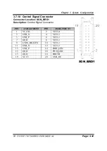
3.7.15 LVDS Connector
Connector Location: LVDS1
Description:
LVDS Connector
PIN
ASSIGNMENT
PIN
ASSIGNMENT
2
GND
1
LVDS_VCC
4
LV
3
LVDS1_CLK-
6
LVDS1_D2-
5
GND
8
GND
7
L
10
L
9
LDVS1_D1-
12
LVDS1_D3-
11
L
14
LVDS1_D0-
13
L
16
LV
15
GND
18
GND
17
LVDS0_CLK-
20
LVDS0_D2-
19
L
22
L
21
GND
24
GND
23
LVDS0_D1-
26
LVDS0_D0-
25
L
28
LVDS0_D3-
27
L
30
LVDS_VCC
29
LVDS_VCC
3.7.16 LVDS Inverter Connector
Connector Location: INV1
Description:
LVDS Inverter Connector
PIN
ASSIGNMENT
1
+12V
2
+12V
3
GND
4
BRCTR
5
GND
6
BKLTEN
LVDS1
INV1
Summary of Contents for SP-7165
Page 9: ...vi Configuring WatchDog Timer B 25 Flash BIOS Update B 27 ...
Page 16: ...Chapter 2 Getting Started SP 7165 SP 7167 SERIES USER MANUAL Page 2 4 Side View ...
Page 19: ...Chapter 2 Getting Started SP 7165 SP 7167 SERIES USER MANUAL Page 2 7 Side View ...
Page 151: ...Appendix B Technical Summary SP 7165 SP 7167 SERIES USER MANUAL Page B 2 System Block Diagram ...
Page 177: ...Appendix B Technical Summary SP 7165 SP 7167 SERIES USER MANUAL Page B 28 ...