background image

PEX 8619BA Base Board RDK Hardware Reference Manual – Version 1.0 
Copyright © 2008 by PLX Technology, Inc. All rights reserved 

14 

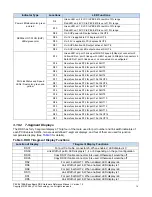
Indicator Type 

Locations 

LED Functions 

Power LEDs/dual color: green 

and red 

D8 

Green LED on: 2.5VCC to PEX 8619 is within 10% range 

Red LED on: 2.5VCC to PEX 8619 is out of 10% range 

D10 

Green LED on: 1.0VCC to PEX 8619 is within 10% range 

Red LED on: 1.0VCC to PEX 8619 is out of 10% range 

SERIAL HOT-PLUG (SHP) 

LEDs/green color 


D28 

On: SHP power LED output active at SLOT 8 

D29 

On: 12V is applied to PCI Express SLOT 8 

D30 

On: 3.3V is applied to PCI Express SLOT 8 

D31 

On: SHP Attention LED output active at SLOT 8 

D32 

On: SHP Interlock LED output active at SLOT 8 

Port Link Status and Speed 

LEDs / Dual color: green and 

yellow 


D12 

Green LED on: port 0 link up with GEN 2 speed (5Gbps) at connector J5 

Yellow LED on: port 0 link up with GEN 1 speed (2.5Gbps) at connector J5 

Both LED off: port 0 link down or no connected or no configured 

D16 

Same function as D12 for port 4 at SLOT1 

D20 

Same function as D12 for port 6 at SLOT2 

D24 

Same function as D12 for port 8 at SLOT3 

D13 

Same function as D12 for port 2 at SLOT4 

D17 

Same function as D12 for port 10 at SLOT5 

D21  

Same function as D12 for port 12 at SLOT6 

D25 

Same function as D12 for port 14 at SLOT7 

D14  

Same function as D12 for port 1 at SLOT8 

D18 

Same function as D12 for port 5 at SLOT9 

D22 

Same function as D12 for port 7 at SLOT10 

D26 

Same function as D12 for port 9 at SLOT11 

D15 

Same function as D12 for port 3 at SLOT12 

D19 

Same function as D12 for port 6 at SLOT13 

D23 

Same function as D12 for port 13 at SLOT14 

D27 

Same function as D12 for port 15 at SLOT15 

3.10.2  7-Segment Displays 

The RDK has forty 7-segment displays. Thrity-four of them are used for port number and link width indicators of 
each PCI Express SLOTs, two are user defined 7-segment displays, and four of them are used for junction 
temperature display. (See 

Table 3

 for details). 

Table 3. RDK 7-Segment Display Functions


Location of Display 

7-Segment Display Functions 

DS37 

For port 0 at cable connector J5, When enabled, LED display is 0 

DS39 

Link Width of port0, LED display is 1, 4 or 8 depending on the port configuration 

DS33 

Copy DS37 if cable connector J6 is used. Otherwise it would be off 

DS35 

Copy DS39 if cable connector J6 is used. Otherwise it would be off 

DS2 

For port 4 at SLOT1, When enabled, LED display is 4 

DS6 

Link Width of port 4, When enabled, LED display is 1 

DS9 

For port 6 at SLOT2, When enabled, LED display is 6 

DS13 

Link Width of port 6, When enabled, LED display is 1 

DS1 

For port 8 at SLOT3, When enabled, LED display is 8 

DS5 

Link Width of port 8, When enabled, LED display is 1 

Summary of Contents for PEX 8619BA

Page 1: ...Base Board RDK Hardware Reference Manual Version 1 0 April 2009 Website www plxtech com Technical Support www plxtech com support Copyright 2009 by PLX Technology Inc All Rights Reserved Version 1 0 April 15 2009 ...

Page 2: ...oduct at any time without notice Products may have minor variations to this publication known as errata PLX assumes no liability whatsoever including infringement of any patent or copyright for sale and use of PLX products PLX Technology and the PLX logo are registered trademarks of PLX Technology Inc Other brands and names are the property of their respective owners Document Number PEX8619BA Base...

Page 3: ...s subject to change without notice Although every effort has been made to ensure the accuracy of this manual PLX shall not be liable for any errors incidental or consequential damages in connection with the furnishing performance or use of this manual or examples herein PLX assumes no responsibility for damage or loss resulting from the use of this manual for loss or claims by third parties which ...

Page 4: ...s 13 3 10 1 LED Indicators 13 3 10 2 7 Segment Displays 14 3 11 GPIO Pins 15 3 12 Reserved Pins 15 4 On Board Connectors Switches and Jumpers 16 4 1 DIP Switches 16 4 1 1 Dip Switch Group 1 16 4 1 2 Dip Switch Group 2 17 4 1 3 Dip Switch Group 3 19 4 2 Push Button Switches 20 4 2 1 Manual Reset S1 20 4 2 2 FPGA Manual Reset S2 20 4 2 3 Serial Hot Plug Controller Attention Button S3 21 4 3 Connecto...

Page 5: ...Figure 19 x4 upstream 12x1 downstream PCFG 0001 28 Figure 20 x4 upstream 1x4 and 8x1 downstream PCFG 0010 29 Figure 21 x4 upstream 2x4 and 4x1 downstream PCFG 0011 30 Figure 22 x8 upstream 8x1 downstream PCFG 0101 31 Figure 23 x8 upstream 1x4 and 4x1 downstream PCFG 0110 32 TABLES Table 1 Port Configurations Supported by the RDK 5 Table 2 RDK LED Indicator descriptions 13 Table 3 RDK 7 Segment Dis...

Page 6: ...nd configurable ports x1 x4 or x8 x2 is also supported Flexible device configuration o Configurable via serial EEPROM I 2 C hardware strapping or by the host Maximum packet payload size of 2 048 bytes Designate any Port as the Upstream Port Port 0 is recommended Dynamic Buffer Pool Architecture Read Pacing allows user to throttle Read requests from Downstream Ports to allow for more efficient perf...

Page 7: ...Figure 1 PEX 8619BA Base Board RDK Front View PEX 8619BA Base Board RDK Hardware Reference Manual Version 1 0 Copyright 2008 by PLX Technology Inc All rights reserved 2 ...

Page 8: ...ture Extensions IEEE Standard 1149 6 2003 o The I2 C Bus Specification Version 2 1 I2 C Bus v2 1 1 2 PEX 8619BA BB RDK Features PLX PEX 8619 PCI Express switch in a 324 ball Plastic BGA package Based on PCI Express Card Electromechanical CEM Specification 2 0 and PCI Express External Cabling Specification 1 0 Supports up to 6 different port configurations with x4 PCI Express cable connection s to ...

Page 9: ...ent of major component blocks on the RDK base board Figure 2 and Figure 3 provide diagrams of the RDK being used in a PC The RDK provides up to 15 PCI Express slots for add in cards and visual indicators for port link status and speed information The RDK is designed to be powered up with an ATX power supply Figure 2 Connecting The RDK to a PC with x1 or x4 link Figure 3 Connecting the RDK to a PC ...

Page 10: ...ettings and the right Configuration Modules are installed the RDK can demonstrate up to 16 ports and a up to x8 link upstream connection PCI Express Gen 2 switch Table 1 shows all port configurations supported by the RDK while sections 3 2 1 to 3 2 5 describe the Configuration Modules and hardware configurations of grouped of each four PCI Express lanes in details Table 1 Port Configurations Suppo...

Page 11: ...press Connectors Port 0 x4 link or lower 4 lanes of x8 link to upstream SLT3 SL2 SLT1 Configuration Module 0107 Lane 0 3 Lane 0 3 4x PCIe Cable Connector J5 U74 U74 PEX 8619 U100 Lane 3 0 Lane 8 11 Lane 4 7 Lane 12 15 A1 A1 PEX 8619 U100 Lane 3 0 Lane 8 11 Lane 4 7 Lane 12 15 a b Figure 4 Lanes 0 3 Hardware Connections on the RDK 3 2 3 PCI Express Lane 4 to Lane 7 PCI Express lanes 4 7 of PEX 8619...

Page 12: ...ted to PCI Express SLOT 8 to SLOT 11 with x1 link each to form ports 1 5 7 and 9 When Configuration Module 0107 is plugged into U76 at Case b four lanes will be connected to SLOT 8 to form a x4 link port 1 x16 PCI Express Connectors x16 PCI Express Connectors Lane 4 7 Lane 12 15 Lane 4 7 Lane 12 15 Figure 6 Lanes 8 11 Hardware Connections on the RDK PEX 8619BA Base Board RDK Hardware Reference Man...

Page 13: ...erminations and voltage dividers The clock circuits are designed to perform two major clock functions reference clock fan out and Spread Spectrum Clock Isolation Refer to Figure 8 the PCI Express clock CREFCLKp and CREFCLKn from x4 PCI Express External Cable Connector J5 feeds into 1 to 4 fan out buffer U28 The outputs from U28 support the primary REFCLK of the PEX 8619 and connect to the inputs o...

Page 14: ... Termination Source Termination Source Termination Source Termination C C C C C C C C C C C C C C C C C Voltage Devider Voltage Devider Voltage Devider Voltage Devider Voltage Devider Voltage Devider SLOT 1 SLOT 2 SLOT 3 SLOT 4 SLOT 5 Voltage Devider Voltage Devider Voltage Devider Voltage Devider Voltage Devider SLOT 6 SLOT 7 SLOT 8 SLOT 9 SLOT 10 Voltage Devider Voltage Devider Voltage Devider V...

Page 15: ...clk VCC P2 SW11 HP_SL8_CTL SHPC_INT VCC Figure 10 SERIAL HOT PLUG Circuits Refer to Figure 10 above the serial Hot Plug controller consists of MAX7311 I O expander U71 a TI TPS2311 dual hot swap power controller U70 a quad TI SN74LVC157 2 to 1 multiplexer U72 two power MOSFET IRF7470 Q1 and Q2 LEDs manual switch dipswitches and resistors The PEX 8619 master I2 C interface is designed for the speci...

Page 16: ...upply is required Refer to Figure 11 the RDK has 8 different ATX power connectors for power connections These include one 24 pin ATX Main Power Connector J9 six 4 pin Peripheral Power Connectors J1 J4 J7 J8 and one 8 pin 12 V Power Connector SLOT15 Figure 11 RDK ATX Power Connectors The 24 pin ATX Power Connector should be connected to J9 and two or three 4 pin ATX Peripheral Power Connectors shou...

Page 17: ... RDK on board circuits and the PEX 8619 get their power from the 5V input from the ATX power supply DC DC converter U4 uses 5V input generates 3 3VCC1 to the on board circuit The 3 3VCC1 further steps down by voltage regulator U117 to generate 2 5V and 1 2V for Xilinx FPGA U115 Three dc dc converters U2 U3 and U5 use 5V input to generate 1 0VCC 1 0VCC_A and 2 5VCC for PEX 8619 Dip switch SW15 can ...

Page 18: ...ED and 7 Segment Displays The RDK provides 31 LEDs and forty 7 segment displays for power indicators Hot Plug output indicators link speed status port numbers and link width of each port 3 10 1 LED Indicators All LED indicators and their associated functions are described in the Table 2 below Table 2 RDK LED Indicator descriptions Indicator Type Locations LED Functions Power LEDs green color D1 On...

Page 19: ...T6 D25 Same function as D12 for port 14 at SLOT7 D14 Same function as D12 for port 1 at SLOT8 D18 Same function as D12 for port 5 at SLOT9 D22 Same function as D12 for port 7 at SLOT10 D26 Same function as D12 for port 9 at SLOT11 D15 Same function as D12 for port 3 at SLOT12 D19 Same function as D12 for port 6 at SLOT13 D23 Same function as D12 for port 13 at SLOT14 D27 Same function as D12 for p...

Page 20: ...LED display is 9 DS21 Link Width of port 9 When enabled LED display is 1 DS28 For port 3 at SLOT12 When enabled LED display is 3 DS32 Link Width of port 3 When enabled LED display is 1 DS20 For port 6 at SLOT13 When enabled LED display is 6 DS24 Link Width of port 6 When enabled LED display is 1 DS27 For port 13 at SLOT14 When enabled LED display is 13 DS31 Link Width of port 13 When enabled LED d...

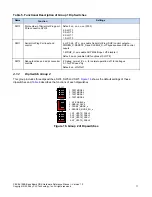
Page 21: ...oup contains five dip switches and is located at the lower right hand corner of the RDK Figure 14 RDK Dip Switch Groups 4 1 1 Dip Switch Group 1 This group includes three dipswitches SW10 SW11 and SW15 Figure 15 shows the default settings of these dipswitches and Table 5 describes the functions of each dipswitches 4 Debug_Normal 3 PLX use only 2 PLX use only 1 PLX use only 2 HP_SL8_CTL 1 MRLI _S 4...

Page 22: ...ion and dc dc converter controls 4 Debug_normal_ on for normal operation off for debug us 3 1 for PLX use only Default on off off off 4 1 2 Dip Switch Group 2 This group includes three dipswitches SW4 SW5 and SW7 Figure 16 shows the default settings of these dipswitches and Table 6 describes the functions of each dipswitches SW7 ON SW5 ON SW4 ON 1 TESTMODE3 2 TESTMODE2 3 TESTMODE1 4 TESTMODE0 1 NT...

Page 23: ... 6 on off off off 7 off on on on 8 off on on off 9 off on off on 10 off on off off 11 off off on on 12 off off on off 13 off off off on 14 off off off off 15 SW5 NT port and debug mode enables 1 NT_ENABLE_n on enable NT mode off disable NT mode default disable NT mode 2 DEBUG_SEL0 for PLX use only 3 PROBE_MODE_n for PLX use only 4 SERDES_MODE_EN_n for PLX use only Default 1 4 off off off off SW7 T...

Page 24: ...G1 4 PORT_CFG0 1 UMODE7 2 UMODE6 3 UMODE5 4 UMODE4 1 UMODE3 2 UMODE2 3 UMODE1 4 UMODE0 Figure 17 Group 3 of Dip Switches Table 7 Port Configurations use Dipswitch SW2 Dipswitch Settings for STRAP_PORTCFG 3 0 Port Configurations ON ON ON ON 0000 x1x1x1x1x1x1x1x1x1x1x1x1x1x1x1x1 ON ON ON OFF 0001 x41x1x1x1x1x1x1x1x1x1x1x1 ON ON OFF ON 0010 x4x41x1x1x1x1x1x1x1 ON ON OFF OFF 0011 x4x4x41x1x1x1 ON OFF ...

Page 25: ...N_n on enable the Spread Spectrum Clocking SSC crossing off disable it default is disable SSC crossing function 2 PP_PYPASS_n for PLX use only 3 GEN 1_N for PLX use only 4 FAST_BRINGUP_n for PLX use only Default 1 4 off off off off SW13 Users Define Mode Switches 1 UMODE3 2 UMODE2 3 UMODE1 4 UMODE0 Default 1 4 off off off off SW14 Users Define Mode Switches 1 UMODE7 2 UMODE6 3 UMODE5 4 UMODE4 Defa...

Page 26: ...Headers 4 3 1 ATX Peripheral Power Connectors J1 J4 J7 J8 The RDK has six ATX Peripheral Power Connectors Table 9 Signal Names of J1 J4 J7 J8 Pin Signal Name 1 12V 2 GND 3 GND 4 5V 4 3 2 x4 PCI Express External Cable Connectors J5 J6 The RDK has two x4 PCI Express External Cable Connectors Table 10 Signal Names of J5 and J6 Pin Signal Name Pin Signal Name A1 GND B1 GND A2 PETp0 B2 PERp0 A3 PETn0 B...

Page 27: ...6 5VDC 18 COM 7 COM 19 COM 8 PWR_OK 20 5VDC 9 5VSB 21 5VDC 10 12VDC 22 5VDC 11 12VDC 23 5VDC 12 3 3VDC 24 COM 4 3 4 ATX 12V Power Connector J10 Table 12 Signal Names of J10 Pin Signal Name Pin Signal Name 1 COM 13 12VDC 2 COM 14 12VDC 3 COM 15 12VDC 4 COM 16 12VDC 4 3 5 Xilinx JTAG Connector J12 Table 13 Signal Names of J12 Pin Signal Name Pin Signal Name 1 VREF to 2 5V 2 GND 3 SS_PROG_TMS 4 GND 5...

Page 28: ...roller The pin assignment for the JTAG header JP3 is listed at Table 15 Table 15 Pin assignment of JP3 Pin Signal Name Pin Signal Name 1 JTAG_TRST 2 GND 3 JTAG_TDI 4 GND 5 JTAG_TDO 6 GND 7 JTAG_TMS 8 GND 9 JTAG_TCK 10 GND 4 3 8 SMBus Header JP5 This header is for PLX use only Table 16 Signal Names of JP5 Pin Signal Name Pin Signal Name 1 SMBCLK 2 GND 3 SMBDATA 4 NC 4 3 9 PCI Express x8 Midbus Prob...

Page 29: ...ownstream 35 GND 38 GND 37 C6p Upstream 40 C6p Downstream 39 C6n Upstream 42 C6n Downstream 41 GND 44 GND 43 C7p Upstream 46 C7p Downstream 45 C7n Upstream 48 C7n Downstream 47 G2 GND 4 3 10 PEX 8619 I2 C Port JP8 Table 18 Pin assignment of JP8 Pin Number Signal Name 1 I2C_SCL0 2 GND 3 I2C_SDA0 4 NC 4 3 11 Debug Signal Header JP9 JP11 This is for PLX use only Table 19 Pin assignment of JP9 JP11 Pi...

Page 30: ...PIO27 35 STRAP_NT_P2P_EN 37 GND 39 GND GND 40 GND GND 41 GND GND 42 GND GND 43 GND GND 2 4 6 8 LN_GOOD_00_n GPIO0 10 LN_GOOD_01_n GPIO1 12 LN_GOOD_02_n GPIO2 14 LN_GOOD_03_n GPIO3 16 LN_GOOD_04_n GPIO4 18 LN_GOOD_05_n GPIO5 20 LN_GOOD_06_n I2C_ADDR0 22 LN_GOOD_07_n I2C_ADDR1 24 LN_GOOD_08_n STRAP_SPARE1 26 LN_GOOD_09_n GPIO9 28 LN_GOOD_10_n GPIO10 30 LN_GOOD_11_n GPIO11 32 LN_GOOD_12_n GPIO12 34 L...

Page 31: ...ment of JP10 Pin Signal Name Pin Signal Name 1 GND 2 STRAP_SPARE1 3 I2C_ADDR2 4 I2C_ADDR1 5 GPIO30 6 I2C_ADDR0 7 GPIO29 8 GND 9 UPSTRM_PSEL3 10 GPIO5 11 STRAP_SPARE0 12 GPIO4 13 GND 14 GPIO3 15 STRAP_SMBUS_EN 16 GPIO2 17 STRAP_UPCFG_TIMER_EN 18 GPIO1 19 DEBUG_SEL0 20 GPIO0 4 3 13 Reference Clock Header JP100 Table 21 Pin assignment of JP100 Pin Number Signal Name 1 LAI_Refclk_p 2 GND 3 LAI_Refclk_...

Page 32: ...W4 ON SW2 ON SW14 ON SW13 ON SW3 ON SW6 ON JP8 1 2 3 4 JP10 1 1 JP3 D1 12V_A D2 5V_A D29 12V_SLT_8_HP D30 3 3VCC_SLT_8_HP D32 Interlock_S D31 ATNLED _S D28 PWRLED _S D3 3 3VCC D9 3 3VCC1 JP6 GND BJ9 BJ10 GND BJ6 BJ5 BJ4 BJ3 GND Midbus Probe Footprint Mictor Connectors Debug Input Header I2C Port JTAG Port 2 5VCC 1 0VCC_A 1 0VCC Port Port Port Link Width Port S1 FPGA JTAG Port Manual Reset FPGA Res...

Page 33: ...Figure 19 x4 upstream 12x1 downstream PCFG 0001 PEX 8619BA Base Board RDK Hardware Reference Manual Version 1 0 Copyright 2008 by PLX Technology Inc All rights reserved 28 ...

Page 34: ...Figure 20 x4 upstream 1x4 and 8x1 downstream PCFG 0010 PEX 8619BA Base Board RDK Hardware Reference Manual Version 1 0 Copyright 2008 by PLX Technology Inc All rights reserved 29 ...

Page 35: ...PEX 8619BA Base Board RDK Hardware Reference Manual Version 1 0 Copyright 2008 by PLX Technology Inc All rights reserved 30 Figure 21 x4 upstream 2x4 and 4x1 downstream PCFG 0011 ...

Page 36: ...PEX 8619BA Base Board RDK Hardware Reference Manual Version 1 0 Copyright 2008 by PLX Technology Inc All rights reserved 31 Figure 22 x8 upstream 8x1 downstream PCFG 0101 ...

Page 37: ...Figure 23 x8 upstream 1x4 and 4x1 downstream PCFG 0110 PEX 8619BA Base Board RDK Hardware Reference Manual Version 1 0 Copyright 2008 by PLX Technology Inc All rights reserved 32 ...

Page 38: ... SN74LVC157AP W IC Quad 2 to 1 data selector multiplexer SMT TSSOP 16 U72 12 1 MAXIM MAX6658MSA IC SMBus compatible temperature sensor SMT SO 8 U78 13 5 NXP SEMI SN74LVC04AD IC hex inverter SMT SO 14 U80 U85 U87 U91 U92 14 1 On Semiconductor NB3N5573DTG IC crystal to HCSL clock generator 3 3V SMT TSSOP 16 U108 15 2 On Semiconductor MC100LVEP111 FAG IC 1 10 differential ECL PECL HSTL clock driver 2...

Page 39: ...R408 40 40 Panasonic ERJ 3GEYJ102V RES 1K OHM 5 SMT 0603 R434 R435 R436 R437 R438 R439 R440 R441 R442 R443 R444 R445 R446 R447 R448 R505 R506 R507 R508 R509 R511 R512 R513 R514 R515 R516 R517 R518 R519 R520 R521 R522 R523 R524 R525 R526 R527 R528 R529 R510 42 40 Panasonic ERJ 3GEYJ121V RES 120 OHM 5 SMT 0805 R530 R531 R532 R533 R534 R535 R536 R537 R538 R539 R540 R541 R542 R543 R544 R545 R546 R547 ...

Page 40: ...M04F10R0CTL F RES 10 0 OHM 1 SMT 0402 R346 61 1 Panasonic ERJ 2RKF1181X RES 1 18K OHM 1 SMT 0402 R41 62 3 Panasonic ERJ 2RKF1201X RES 1 21K OHM 1 SMT 0402 R1 R12 R252 63 1 Panasonic ERJ 2RKF1242X RES 12 4K OHM 1 SMT 0402 R249 64 1 Panasonic ERJ 2RKF1372X RES 13 7K OHM 1 SMT 0402 R250 65 3 Panasonic ERJ 2RKF1500X RES 150 OHM 1 SMT 0402 R253 R255 R256 66 1 Yageo RM04F2000CTL F RES 200 OHM 1 SMT 0402...

Page 41: ... 0805 C1 C2 C6 C8 C10 C12 C13 C16 C19 C20 C21 C24 C25 C26 C27 C28 C44 C46 C48 C63 C65 C71 C161 C257 C296 C298 C301 C302 C305 C306 C308 C310 96 2 Kemet GMC21X5R106 M6R3NT CAP 10uf 6 3V 20 X5R SMT 0805 C75 C84 97 1 CALCHIP 08055C223KAT 2A CAP 0 022uf 50V 10 X7R SMT 0805 C163 98 1 CALCHIP GMC21X5R226 M6R3NT CAP 22uf 6 3V 20 X5R SMT 0805 C156 99 1 AVX 06033A180GAT 2A CAP 18PF 25V NP0 SMT 0603 C327 100...

Page 42: ...96 C97 C99 C100 C129 C130 C134 C135 C136 C138 108 20 Panasonic ECJ ZEB1E102K CAP 1000PF 25V X7R SMT 0201 C103 C104 C111 C112 C113 C114 C115 C119 C131 C132 C139 C140 C142 C143 C144 C147 C149 C150 C152 C155 109 3 Vishay 594D187X0016 R2T CAP 180UF 16V 20 Tantalum SMT D Case C34 C35 C36 THROUGH HOLE COMPONENTS 200 40 Lumex LDS A516RI 7 SEGMENT display red common anode 0 75 x0 48 10 pin DIP DS1 DS2 DS3...

Page 43: ...9 Base Board RDK PART THAT SHOULD NOT BE ASSEMBLED 500 0 Concord Electronics 09 9127 1 0210 CONN banana jack black color TH BJ3 BJ6 BJ9 501 0 Concord Electronics 09 9127 1 0212 CONN banana jack red color TH BJ4 BJ5 BJ10 502 0 Agilent E5387 68701 Midbus LAI 48 pin header shroud TH JP6 503 0 TBD TBD RES SMT 2512 R15 R18 R18 R19 R20 R21 R22 R23 R24 R25 R26 R27 R36 R39 R40 R46 R48 R51 R52 R55 504 0 Ma...

Page 44: ... 2009 www plxtech com 8619 Base Board RDK Title Size Document Number Rev Date Sheet of 91 0131 000 A 0 PLX TECHNOLOGY INC 870 W Maude Ave Sunnyvale CA 94085 C 1 26 Thursday February 12 2009 www plxtech com 8619 Base Board RDK x1 SLOT1 x1 x1 SLOT2 SLOT3 x1 x1 SLOT5 SLOT6 x1 SLOT7 x1 SLOT4 x1 x1 SLOT9 SLOT10 x1 SLOT11 x1 SLOT8 x1 x1 SLOT13 SLOT14 x1 SLOT15 x1 SLOT12 CONFIG RECEPTACLE EPROM PORT ID P...

Page 45: ...oard RDK Title Size Document Number Rev Date Sheet of 91 0131 000 A 0 PLX TECHNOLOGY INC 870 W Maude Ave Sunnyvale CA 94085 C 2 26 Monday March 09 2009 www plxtech com 8619 Base Board RDK RELEASE NOTES Initial Release Apr 18 2008 Release 0 1 May 15 2008 changed the RefClock Fanout Buffer to MC100LVEP111 Chnaged the Xilinx FPGA part from XCS40XL to XC3S200 and the associated prom Added the Multiout...

Page 46: ...8619 Base Board RDK Title Size Document Number Rev Date Sheet of 91 0131 000 A 0 PLX TECHNOLOGY INC 870 W Maude Ave Sunnyvale CA 94085 C 3 26 Thursday February 12 2009 www plxtech com 8619 Base Board RDK Title Size Document Number Rev Date Sheet of 91 0131 000 A 0 PLX TECHNOLOGY INC 870 W Maude Ave Sunnyvale CA 94085 C 3 26 Thursday February 12 2009 www plxtech com 8619 Base Board RDK RELEASE NOTE...

Page 47: ...7AH 08E1A0 Vin 2 Vout 4 On Off 1 Gnd 3 Trim 5 NC0 6 NC1 7 BJ10 red BJ10 red 1 C19 1uF C19 1uF C4 22uF C4 22uF J10 ATX 4plus4 Proc 12V Conn J10 ATX 4plus4 Proc 12V Conn GND1 1 GND2 2 GND3 3 GND4 4 12V1_1 5 12V1_2 6 12V2_1 7 12V2_2 8 D2 GREEN D2 GREEN 2 1 D3 GREEN D3 GREEN 2 1 TV12 Prototyping Pad TV12 Prototyping Pad C36 180uF C36 180uF TV19 Prototyping Pad TV19 Prototyping Pad TV46 Prototyping Pad...

Page 48: ...60 20K R308 5 1K R308 5 1K R329 33 R329 33 R336 5 1K R336 5 1K R314 0 Shunt R314 0 Shunt 1 2 3 R301 33 R301 33 R316 33 R316 33 U98 NL U98 NL NC0 7 NC1 8 NC2 9 NC3 10 OE 1 RREF 2 GND 3 VCC 6 OUTN 5 OUTP 4 RN55 4R 4 7K RN55 4R 4 7K 1 2 3 4 5 6 7 8 R289 33 R289 33 U61 CY28400 2 U61 CY28400 2 VDD0 1 VDD1 5 VDD2 11 VDD3 18 VDD4 24 VSS 4 OE_INV 25 VDD_A 28 VSS_A 27 SRC_IN 2 SRC_IN 3 OE_1 8 OE_6 21 HIGH_...

Page 49: ... 0 1uF C493 0 1uF R469 10K R469 10K R540 120 R540 120 R510 1K R510 1K R451 7 32K R451 7 32K C476 0 1uF C476 0 1uF C494 0 1uF C494 0 1uF R541 120 R541 120 R550 120 R550 120 R435 1K R435 1K R460 10K R460 10K R530 120 R530 120 R444 1K R444 1K R525 1K R525 1K R468 10K R468 10K R458 10K R458 10K R496 10K R496 10K R535 120 R535 120 R464 7 32K R464 7 32K R455 10K R455 10K C336 10uF C336 10uF C492 0 1uF C...

Page 50: ...2 1 43K 1 R282 1 43K 1 C267 0 1uF C267 0 1uF C285 0 1uF C285 0 1uF C273 0 1uF C273 0 1uF C268 0 1uF C268 0 1uF TV35 Prototyping Pad TV35 Prototyping Pad C286 0 1uF C286 0 1uF C274 0 1uF C274 0 1uF JP100 TMS 103 02 S S JP100 TMS 103 02 S S REFCLK 1 REFCLK 3 GND 2 C264 0 1uF C264 0 1uF TV37 Prototyping Pad TV37 Prototyping Pad R283 1 43K 1 R283 1 43K 1 C283 0 1uF C283 0 1uF C271 0 1uF C271 0 1uF TV4...

Page 51: ...SS31 G7 VSS30 G5 VSS29 G4 VSS28 G3 VSS27 G2 VSS26 G1 VSS25 F18 VSS24 F17 VSS23 F16 VSS22 F15 VSS21 F14 VSS20 F10 VSS19 F5 VSS18 E12 VSS17 E6 VSS16 D12 VSS15 D6 VSS14 C12 VSS11 C6 VSS61 L7 VSS63 L9 VSS65 L11 VSS67 M7 VSS68 M8 VSS70 M10 VSS71 M11 VSS62 L8 VSS64 L10 VSS66 L12 VSS69 M9 VSS72 M12 VSS73 M14 VSS74 M15 VSS75 M16 VSS76 M17 VSS77 M18 VSS78 N1 VSS79 N2 VSS80 N3 VSS81 N4 VSS82 N5 VSS83 N9 VSS...

Page 52: ...6 B42 GND15 B43 GND16 B44 PETp7 B45 PETn7 B46 GND17 B47 PRSNT2 _2 B48 GND18 B49 PETp8 B50 PETn8 B51 GND19 B52 GND20 B53 PETp9 B54 PETn9 B55 GND21 B56 GND22 B57 PETp10 B58 PETn10 B59 GND23 B60 PERn10 A61 GND57 A62 GND58 A63 PERp11 A64 PERn11 A65 GND59 A66 GND60 A67 PERp12 A68 PERn12 A69 GND61 A70 GND62 A71 PERp13 A72 PERn13 A73 GND63 A74 GND64 A75 PERp14 A76 PERn14 A77 GND65 A78 GND66 A79 PERp15 A8...

Page 53: ...A57 GND55 A58 GND56 A59 PERp10 A60 PRSNT2 _1 B31 GND10 B32 PETp4 B33 PETn4 B34 GND11 B35 GND12 B36 PETp5 B37 PETn5 B38 GND13 B39 GND14 B40 PETp6 B41 PETn6 B42 GND15 B43 GND16 B44 PETp7 B45 PETn7 B46 GND17 B47 PRSNT2 _2 B48 GND18 B49 PETp8 B50 PETn8 B51 GND19 B52 GND20 B53 PETp9 B54 PETn9 B55 GND21 B56 GND22 B57 PETp10 B58 PETn10 B59 GND23 B60 PERn10 A61 GND57 A62 GND58 A63 PERp11 A64 PERn11 A65 GN...

Page 54: ...D55 A58 GND56 A59 PERp10 A60 PRSNT2 _1 B31 GND10 B32 PETp4 B33 PETn4 B34 GND11 B35 GND12 B36 PETp5 B37 PETn5 B38 GND13 B39 GND14 B40 PETp6 B41 PETn6 B42 GND15 B43 GND16 B44 PETp7 B45 PETn7 B46 GND17 B47 PRSNT2 _2 B48 GND18 B49 PETp8 B50 PETn8 B51 GND19 B52 GND20 B53 PETp9 B54 PETn9 B55 GND21 B56 GND22 B57 PETp10 B58 PETn10 B59 GND23 B60 PERn10 A61 GND57 A62 GND58 A63 PERp11 A64 PERn11 A65 GND59 A6...

Page 55: ...ND11 B35 GND12 B36 PETp5 B37 PETn5 B38 GND13 B39 GND14 B40 PETp6 B41 PETn6 B42 GND15 B43 GND16 B44 PETp7 B45 PETn7 B46 GND17 B47 PRSNT2 _2 B48 GND18 B49 PETp8 B50 PETn8 B51 GND19 B52 GND20 B53 PETp9 B54 PETn9 B55 GND21 B56 GND22 B57 PETp10 B58 PETn10 B59 GND23 B60 PERn10 A61 GND57 A62 GND58 A63 PERp11 A64 PERn11 A65 GND59 A66 GND60 A67 PERp12 A68 PERn12 A69 GND61 A70 GND62 A71 PERp13 A72 PERn13 A7...

Page 56: ...7 B47 PRSNT2 _2 B48 GND18 B49 PETp8 B50 PETn8 B51 GND19 B52 GND20 B53 PETp9 B54 PETn9 B55 GND21 B56 GND22 B57 PETp10 B58 PETn10 B59 GND23 B60 PERn10 A61 GND57 A62 GND58 A63 PERp11 A64 PERn11 A65 GND59 A66 GND60 A67 PERp12 A68 PERn12 A69 GND61 A70 GND62 A71 PERp13 A72 PERn13 A73 GND63 A74 GND64 A75 PERp14 A76 PERn14 A77 GND65 A78 GND66 A79 PERp15 A80 PERn15 A81 GND67 A82 GND24 B61 PETp11 B62 PETn11...

Page 57: ...Tn7 B46 GND17 B47 PRSNT2 _2 B48 GND18 B49 PETp8 B50 PETn8 B51 GND19 B52 GND20 B53 PETp9 B54 PETn9 B55 GND21 B56 GND22 B57 PETp10 B58 PETn10 B59 GND23 B60 PERn10 A61 GND57 A62 GND58 A63 PERp11 A64 PERn11 A65 GND59 A66 GND60 A67 PERp12 A68 PERn12 A69 GND61 A70 GND62 A71 PERp13 A72 PERn13 A73 GND63 A74 GND64 A75 PERp14 A76 PERn14 A77 GND65 A78 GND66 A79 PERp15 A80 PERn15 A81 GND67 A82 GND24 B61 PETp1...

Page 58: ...5 B38 GND13 B39 GND14 B40 PETp6 B41 PETn6 B42 GND15 B43 GND16 B44 PETp7 B45 PETn7 B46 GND17 B47 PRSNT2 _2 B48 GND18 B49 PETp8 B50 PETn8 B51 GND19 B52 GND20 B53 PETp9 B54 PETn9 B55 GND21 B56 GND22 B57 PETp10 B58 PETn10 B59 GND23 B60 PERn10 A61 GND57 A62 GND58 A63 PERp11 A64 PERn11 A65 GND59 A66 GND60 A67 PERp12 A68 PERn12 A69 GND61 A70 GND62 A71 PERp13 A72 PERn13 A73 GND63 A74 GND64 A75 PERp14 A76 ...

Page 59: ... Pad C209 22uF C209 22uF TV32 Prototyping Pad TV32 Prototyping Pad J5 PCIex4_Cab Con J5 PCIex4_Cab Con GND7 B1 GND6 A1 PERp0 B2 PERn0 B3 GND8 B4 PERp1 B5 PERn1 B6 GND9 B7 PERp2 B8 PERn2 B9 GND10 B10 PERp3 B11 PERn3 B12 GND11 B13 PWR0 B14 PWR1 B15 PWR_RTN0 B16 PWR_RTN1 B17 CWAKE B18 CPERST B19 PETp0 A2 PETn0 A3 GND5 A4 PETp1 A5 PETn1 A6 GND4 A7 PETp2 A8 PETn2 A9 GND3 A10 PETp3 A11 PETn3 A12 GND1 A1...

Page 60: ...8 C212 0 01uF C212 0 01uF DS10 Red DS10 Red A 7 B 6 C 4 D 2 E 1 F 9 G 10 DP 5 ANODE0 3 ANODE1 8 C223 0 01uF C223 0 01uF U36 MM74HC164 U36 MM74HC164 GND 7 CLK 8 CLR 9 VCC 14 QA 3 QB 4 QC 5 QD 6 QE 10 QF 11 QG 12 QH 13 A 1 B 2 C213 0 01uF C213 0 01uF C221 0 01uF C221 0 01uF U80E 74LVC04 SO U80E 74LVC04 SO 11 10 DS5 Red DS5 Red A 7 B 6 C 4 D 2 E 1 F 9 G 10 DP 5 ANODE0 3 ANODE1 8 U37 MM74HC164 U37 MM7...

Page 61: ... 13 A 1 B 2 RN40 220 RN40 220 1 2 3 4 5 6 7 8 9 10 11 12 13 14 15 16 RN31 220 RN31 220 1 2 3 4 5 6 7 8 9 10 11 12 13 14 15 16 RN37 220 RN37 220 1 2 3 4 5 6 7 8 9 10 11 12 13 14 15 16 U56 MM74HC164 U56 MM74HC164 GND 7 CLK 8 CLR 9 VCC 14 QA 3 QB 4 QC 5 QD 6 QE 10 QF 11 QG 12 QH 13 A 1 B 2 DS31 Red DS31 Red A 7 B 6 C 4 D 2 E 1 F 9 G 10 DP 5 ANODE0 3 ANODE1 8 U48 MM74HC164 U48 MM74HC164 GND 7 CLK 8 CL...

Page 62: ... 220 1 2 3 4 5 6 7 8 9 10 11 12 13 14 15 16 DS33 Red DS33 Red A 7 B 6 C 4 D 2 E 1 F 9 G 10 DP 5 ANODE0 3 ANODE1 8 U83 MM74HC164 U83 MM74HC164 GND 7 CLK 8 CLR 9 VCC 14 QA 3 QB 4 QC 5 QD 6 QE 10 QF 11 QG 12 QH 13 A 1 B 2 C248 0 01uF C248 0 01uF DS38 Red DS38 Red A 7 B 6 C 4 D 2 E 1 F 9 G 10 DP 5 ANODE0 3 ANODE1 8 C311 0 01uF C311 0 01uF U64 MM74HC164 U64 MM74HC164 GND 7 CLK 8 CLR 9 VCC 14 QA 3 QB 4 ...

Page 63: ... STSx x The PEX_LN0_XpxG should be placed with the close to Port ID Port STS LED for the PCIe Receptacle R230 390 R230 390 G Y D19 GREEN_AMBER_LED G Y D19 GREEN_AMBER_LED 2 1 4 3 R241 390 R241 390 R235 390 R235 390 R225 390 R225 390 R247 390 R247 390 R217 390 R217 390 G R D12 GREEN_AMBER_LED G R D12 GREEN_AMBER_LED 2 1 4 3 R240 390 R240 390 R224 390 R224 390 G Y D20 GREEN_AMBER_LED G Y D20 GREEN_A...

Page 64: ... 51 R267 51 R250 13 7K 1 R250 13 7K 1 D29 GREEN D29 GREEN 2 1 R264 0 02 1 R264 0 02 1 D30 GREEN D30 GREEN 2 1 Q2 IRF7470PBF Q2 IRF7470PBF D0 5 D1 6 D2 7 D3 8 S0 1 S1 2 S2 3 G 4 D31 GREEN D31 GREEN 2 1 R253 150 R253 150 R262 2K R262 2K R263 2K R263 2K C255 0 1uF C255 0 1uF R269 0 R269 0 R274 4 7K R274 4 7K U71 MAX7311AUG U71 MAX7311AUG SCL 22 AD2 3 AD0 21 AD1 2 SDA 23 V 24 INT 1 GND 12 IO0 4 IO1 5 ...

Page 65: ...ceptacle 10 x 20 TX0_S_p A3 TX0_D0_p B3 TX0_D1_p A2 TX0_D2_p B2 TX0_D0_n D3 TX0_D1_n C2 TX0_D2_n D2 TX0_S_n C3 TX1_S_p A7 TX1_S_n C7 TX1_D0_p B7 TX1_D1_p A6 TX1_D2_p B6 TX1_D0_n D7 TX1_D1_n C6 TX1_D2_n D6 TX2_D0_p B11 TX2_D1_p A10 TX2_D2_p B10 TX2_D0_n D11 TX2_D1_n C10 TX2_D2_n D10 TX3_D0_p B15 TX3_D1_p A14 TX3_D2_p B14 TX3_D0_n D15 TX3_D1_n C14 TX3_D2_n D14 TX4_D0_p B19 TX4_D1_p A18 TX4_D2_p B18 ...

Page 66: ... 1000pf C79 1000pf C153 0 001uF C153 0 001uF C384 0 01uF C384 0 01uF R359 10K R359 10K C424 0 01uF C424 0 01uF C382 1000pF C382 1000pF R340 0 Shunt R340 0 Shunt 1 2 3 U21 NC7S08 U21 NC7S08 VCC 5 GND 3 A 1 B 2 Y 4 R62 0 R62 0 C378 1000pF C378 1000pF RN56 10K RN56 10K 1 2 3 4 5 6 7 8 C415 1000pF C415 1000pF C401 1000pF C401 1000pF C385 0 01uF C385 0 01uF C157 0 1uF C157 0 1uF C81 1uF NL C81 1uF NL C...

Page 67: ... B5 GND13 B8 GND14 B9 GND15 B12 GND16 B13 GND17 B16 GND18 B17 GND19 B20 GND20 C1 GND21 C4 GND22 C5 GND23 C8 GND24 C9 GND25 C12 GND26 C13 GND27 C16 GND28 C17 GND29 C20 GND30 D1 GND31 D4 GND32 D5 GND33 D8 GND34 D9 GND35 D12 GND36 D13 GND37 D16 GND38 D17 GND39 D20 GND40 G1 GND41 G4 GND42 G5 GND43 G8 GND44 G9 GND45 G12 GND46 G13 GND47 G16 GND48 G17 GND49 G20 GND50 H1 GND51 H4 GND52 H5 GND53 H8 GND54 H...

Page 68: ...otyping Pad TV70 Prototyping Pad JP11 MICTOR 38 RECEPT JP11 MICTOR 38 RECEPT NC0 1 NC1 2 GND0 3 NC2 4 CLK Q0 5 CLK Q1 6 L3 7 7 R1 7 8 L3 6 9 R1 6 10 L3 5 11 R1 5 12 L3 4 13 R1 4 14 L3 3 15 R1 3 16 L3 2 17 R1 2 18 L3 1 19 R1 1 20 L3 0 21 R1 0 22 L2 7 23 R0 7 24 L2 6 25 R0 6 26 L2 5 27 R0 5 28 L2 4 29 R0 4 30 L2 3 31 R0 3 32 R0 2 34 R0 1 36 R0 0 38 GND2 40 GND4 42 L2 2 33 L2 1 35 L2 0 37 GND1 39 GND...

Page 69: ...GND17 J8 GND18 J9 GND19 J10 GND20 J15 GND21 K7 GND22 K8 GND23 K9 GND24 K10 GND25 L6 GND26 L11 GND27 R2 GND28 R8 GND29 R15 GND30 T1 GND31 T16 RN11 4R 4 7K RN11 4R 4 7K 1 2 3 4 5 6 7 8 TP21 TP21 TP12 ROM_OE_RESET_n TP12 ROM_OE_RESET_n R77 5 1K R77 5 1K RN13 4R 4 7K RN13 4R 4 7K 1 2 3 4 5 6 7 8 TP34 TP34 XC3S200 4FTG256C 6 OF 12 U115F XC3S200 4FTG256C XC3S200 4FTG256C 6 OF 12 U115F XC3S200 4FTG256C I...

Reviews: