56
MEH-P5350
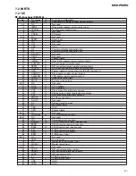
No. Symbol I/O Explain
1 STIND
O
stereo
"Low" when the FM stereo signals are received.
indicator
To be pulled up to the "VDD" at 47k
Ω
.
2 FMSD
O
FM station
"High" when signals are received. To be pulled up to the "VDD" at 47k
Ω
detector
Meanwhile, 10k
Ω
should be used when taking diver FIX trigger from here
and "High: 0.9VDD or more" and "Low: 250mV or less".
(Should satisfy the diver IC specifications)
3 NL1
O
noise level-1
"High" when noise is received. Output for the RDS. GND at 47k
Ω
//1,800pF.
4 NL2
O
noise level-2
"High" when noise is received. Output for the RDS. GND at 36k
Ω
//330pF.
5 Rch
O
R channel
FM stereo "R-ch" signal output or AM audio output.
output
Add the specified di-emphasis constant.
6 Lch
O
L channel
FM stereo "L-ch" signal output or AM audio output.
output
Add the specified di-emphasis constant.
7 WC
write control
EEPROM write control. Writing permissible at "Low". Normally open.
8 SDBW
O
SD bandwidth
SD bandwidth signal output. For detection of detuning data for the RDS.
9 NC
Not used
10 VDD
power
Power supply pin for the digital section.
supply
D.C. 5V +/- 0.25V. Be careful about overlapping noise in the logic section.
11 DGND
digital ground
Grounding for the digital section.
12 CE2
I
chip enable-2
EEPROM chip enable. Active a "Low"
To be pulled up to the "VDD" at 47k
Ω
13 SL
I/O signal level
Received FM/AM signal level (strength) output.
Connect the specified load resistor and capacitor (10k
Ω
+ 39k
Ω
//4,700pF)
14 DI/DO
I/O data input/
Data input/Data output
data output
To be pulled up to the "VDD" at 47k
Ω
15 CK
I
clock
Clock input To be pulled up to the "VDD" at 47k
Ω
16 CE1
I
chip enable-1
AF·RF chip enable. Active at "High" To be grounded at 47k
Ω
17 NC
Not used
18 LDET
O
lock detector
Active at "Low". To be pulled up to the "VDD" at 47k
Ω
19 CREQ
I
current request
Active at "Low". To be grounded at 47k
Ω
20 NC
Not used
21 COMP
O
composite signal
FM composite signal output. r out < 100
Ω
22 VCC
power supply
Analog section power supply pin.D.C.8.4V +/- 0.3V
23 LOCH
I
local high
FM local high pin. When seeking local high, apply 5V together with "LOCL".
24 FMLOCL I
FM local low
FM local low pin. When seeking local low, apply 5V to the base of the NPN
transistor with which the specified resistor is being connected to the emitter.
Keep it open in case of ordinary marketed models.
25 LOCL
I
local low
FM/AM local low pin. When seeking local low, apply 5V to the base of the
NPN transistor. Since this pin is exclusive for AM when the FMLOCL is in use,
do not drive it under FM.
26 RFGND
RF ground
Grounding for the antenna section.
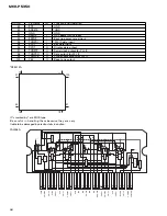
27 FMANT I
FM antenna input FM antenna input. 75
Ω
. Serge absorber (DSP-201M-S00B) is necessary.
28 AMANT I
AM antenna input AM antenna input. High impedance.
Connect to the antenna through an L (LAU type) of 4.7µH.To cope with the
power transmission line hums, insert a series circuit consisting of an L
(a coil of about 100mH) + R (a resistor of 470
Ω
to 2.2k
Ω
) between the GND.
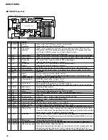
IC 3
EEPROM
FM/AM TUNER UNIT
28
27
FM/AM 1ST IF 10.7MHz
T51 Q51 CF51 CF52 CF53
IC1
MIXER, IF AMP, DET.
6
21
18
LDET
COMP
22
25
10
14
12 15 16
8
13
2
3
4
CF202
VDD
VCC
DI/DO
CE2
CK
CE1
SDBW
SL
FMSD
NL1
NL2
IC 2 FM MPX
AMANT
FMANT
ATT
ATT
AMRF
FMRF
IMG ADJ
RF ADJ
X901
10.25MHz
ANT ADJ
LOCL
23
LOCH
AMDET
MPXREF 41kHz
AM 2ND IF
450kHz
19
CREQ
11
DGND
1
STIND
L ch
5
R ch
9
24
NC
FMLOCL
20
17
7
NC
NC
WC
26
RFGND
-
FM/AM Tuner Unit
Summary of Contents for MEH-P5350
Page 4: ...4 MEH P5350 2 2 EXTERIOR A B ...
Page 6: ...C D E 6 MEH P5350 2 3 MD MECHANISM MODULE ...
Page 16: ...KEY MICROCOMPUTER RESET 560 R47 2R7K 16 MEH P5350 1 2 3 4 1 2 3 4 D C B A 3 3 KEYBOARD UNIT B ...
Page 17: ...B LCD BACK LIGTH B A KEYBOARD UNIT CN831 17 MEH P5350 5 6 7 8 5 6 7 8 D C B A ...
Page 30: ...30 MEH P5350 1 2 3 4 1 2 3 4 D C B A A A TUNER AMP UNIT ...
Page 31: ...31 MEH P5350 5 6 7 8 5 6 7 8 D C B A A SIDE B ...
Page 33: ...33 MEH P5350 1 2 3 4 1 2 3 4 D C B A A CN831 B B SIDE B KEYBOARD UNIT ...
Page 35: ...IC Q D 35 MEH P5350 D C B A 1 2 3 4 1 2 3 4 C MD UNIT C SIDE B ...
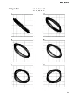
Page 43: ...43 MEH P5350 Grating waveform 45 0 75 60 30 90 Ech Xch 50mV div AC Fch Ych 50mV div AC ...

