background image

100

FH-P4000,P4000R

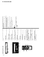
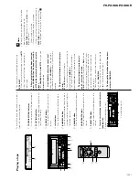
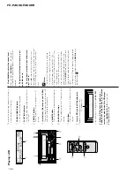
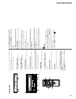
Listening to the radio

These are the basic steps necessar

y to operate

the radio

.

1

BAND

indicator

Shows which band the radio is tuned to

, AM

or FM.

2

STEREO

(

) indicator 

Shows that the frequency selected is being

broadcast in stereo

.

3

FREQUENCY

indicator

Shows to which frequency the tuner is

tuned.

4

2

/

3

buttons (Manual or seek tuning)

P

ress to tune in a radio station

.

5

BAND/ES

C

button

P

ress to select among three FM and one AM

band.

6

VOL

UME 

button

P

ress to increase or decrease the volume.

7

SOURCE/OFF

button

P

ress to select the tuner as the source.

8

TUNER

button

P

ress to select the tuner as the source.

1

P

ress 

SOURCE/OFF

on the head unit, or

TUNER

on the r

emote, to select the tuner

.

P

ress 

SOURCE/OFF

or 

TUNER

until you see

T

uner

displayed.

2

Use 

VOL

UME 

to adjust the sound level.

When you press 

VOL

UME

up/+, the volume is

raised and when pressed down/–, the volume is

lowered.

3

P

ress 

BAND/ES

C

to select a band

.

P

ress 

BAND/ES

C

until the desired band is dis-

played, 

F1

F2

F3

or 

AM

.

4

6

8

5

ENTENT

DISPDISP

CLOCKCLOCK

LOUDLOUD

SOURCESOURCE

/  OFF/  OFF

6

5

4

3

2

1

F

D

A

75

6

4

1

3

2

4

T

o perfor

m manual tuning, pr

ess 

2

or 

3

with quick pr

esses.

The frequencies move up or down step by step.

5

T

o perfor

m seek tuning, pr

ess and hold 

2

or 

3

for about one second and r

elease.

The tuner will scan the frequencies until a

broadcast strong enough for good reception is

found.

You can cancel seek tuning by pressing either

2

or 

3

with a quick press.

If you press and hold 

2

or 

3

you can skip

broadcasting stations. Seek tuning starts as

soon as you release the buttons.

Note

When the frequency selected is being broad-

cast in stereo the 

STEREO 

(

)

indicator will

light. 

Summary of Contents for FH-P4000

Page 1: ...ECTION DIAGRAM 40 5 ELECTRICAL PARTS LIST 50 6 ADJUSTMENT 67 7 GENERAL INFORMATION 72 7 1 DIAGNOSIS 72 7 1 1 TEST MODE 72 7 1 2 DISASSEMBLY 76 7 1 3 CONNECTOR FUNCTION DESCRIPTION 80 7 2 PARTS 81 7 2 1 IC 81 7 2 2 DISPLAY 96 7 3 OPERATIONAL FLOW CHART 97 8 OPERATIONS AND SPECIFICATIONS 98 FH P4000R X1N EW FH P4000 X1N UC This service manual should be used together with the following manual s Model...

Page 2: ... replacement handling precautions shall be taken to prevent an electrostatic discharge protection by a jumper solder 2 During disassembly be sure to turn the power off since an internal IC might be destroyed when a con nector is plugged or unplugged 3 Please checking the grating after changing the ser vice pickup unit see page 70 ...

Page 3: ...ters CLASS 1 LASER PRODUCT CAUTION This service manual is intended for qualified service technicians it is not meant for the casual do it yourselfer Qualified technicians have the necessary test equipment and tools and have been trained to properly and safely repair complex products such as those covered by this manual Improperly performed repairs can adversely affect the safety and reliability of...

Page 4: ...3 Owner s Manual See Contrast table 2 14 4 Installation Manual See Contrast table 2 14 5 Panel See Contrast table 2 14 6 Owner s Manual See Contrast table 2 14 7 Installation Manual See Contrast table 2 14 8 Passport See Contrast table 2 14 9 Warranty Card See Contrast table 2 15 Remote Control Unit See Contrast table 2 16 Cover See Contrast table 2 Mark No Description Part No Mark No Description ...

Page 5: ...LE FH P4000 X1N UC FH P4000R X1N EW and FH P4000 X1N ES are constructed the same except for the following Owner s Manual Installation Manual Model Part No Language FH P4000 X1N UC CRD3403 English French CRD3404 English French FH P4000R X1N EW CRD3397 English Italian Spanish CRD3398 English Italian Spanish CRD3399 French Dutch German CRD3400 French Dutch German FH P4000 X1N ES CRD3401 English Spani...

Page 6: ...6 FH P4000 P4000R 2 2 EXTERIOR FH P4000 X1N UC A B There is a possibility of damaging screws if the torque for tightning the screw indicat ed by arrows more than 0 6N Keep the designated torque ...

Page 7: ...V6585 42 Panel Unit CXB7289 43 Button CAC6904 44 Door CAT2223 45 Spring CBH1838 46 Spring CBH2182 47 Cover CNM6276 48 49 Screw IMS20P040FZK 50 Detach Grille Assy CXB6688 51 Screw BPZ20P080FZK 52 Button CD EJ CAC6889 53 Button VOLUME CAC6890 54 Button 1 6 CAC6891 55 Button SOURCE CAC6892 56 Button TAPE EJ CAC6894 57 Button SEL CAC6896 58 Button LOUD CAC6900 59 Button DISP CAC6901 60 Button DETACH C...

Page 8: ...8 FH P4000 P4000R 2 3 EXTERIOR FH P4000R X1N EW A B There is a possibility of damaging screws if the torque for tightning the screw indicat ed by arrows more than 0 6N Keep the designated torque ...

Page 9: ...it CXB7289 43 Button CAC6904 44 Door CAT2223 45 Spring CBH1838 46 Spring CBH2182 47 Cover CNM6276 48 49 Screw IMS20P040FZK 50 Detach Grille Assy CXB6686 51 Screw BPZ20P080FZK 52 Button CD EJ CAC6889 53 Button VOLUME CAC6890 54 Button 1 6 CAC6891 55 Button SOURCE CAC6892 56 Button TAPE EJ CAC6894 57 Button SEL CAC6896 58 Button TA CAC6899 59 Button DISP CAC6902 60 Button DETACH CAC6903 61 Badge CAH...

Page 10: ...10 FH P4000 P4000R 2 4 EXTERIOR FH P4000 X1N ES B A There is a possibility of damaging screws if the torque for tightning the screw indicat ed by arrows more than 0 6N Keep the designated torque ...

Page 11: ...20P080FZK 33 Button CD EJ CAC6889 34 Button VOLUME CAC6890 35 Button 1 6 CAC6891 36 Button SOURCE CAC6892 37 Button TAPE EJ CAC6894 38 Button SEL CAC6896 39 Button LOUD CAC6898 40 Button DISP CAC6901 41 Badge CAH1792 42 Cover CNM7086 43 Lighting Conductor CNV6577 44 Lighting Conductor CNV6578 45 Guide CNV6580 46 Keyboard Unit CWM7530 47 LCD LCD1000 CAW1664 48 Connector CN1000 CKS3580 49 Holder CNC...

Page 12: ...12 FH P4000 P4000R 2 5 CD MECHANISM MODULE C ...

Page 13: ...51 36 Arm CNC9016 37 Arm CNC9017 38 Bracket CNC9123 39 Frame CNC9263 40 Belt CNT1086 41 Gear CNV6315 42 Gear CNV6316 43 Gear CNV6317 44 Gear CNV6318 45 Gear CNV6319 46 Gear CNV6320 47 Arm CNV6322 48 Arm CNV6323 49 Arm CNV6324 50 Arm CNV6325 51 Arm CNV6326 52 Guide CNV6327 53 Arm CNV6328 54 Guide CNV6329 55 Rack CNV6330 56 Clamper CNV6331 57 Arm CNV6332 58 Guide CNV6333 59 Cover CNV6334 60 Arm CNV6...

Page 14: ...14 FH P4000 P4000R 2 6 CASSETTE MECHANISM MODULE E D ...

Page 15: ...60 30 Worm Wheel ENV1566 31 Lever ENV1551 32 Flywheel ENV1554 33 Gathering PCB ENX1068 34 Switch S1 S2 S3 ESG1007 35 Deck Unit EWM1033 36 Plug CN251 CKS3540 37 Gathering PCB ENX1067 38 Motor Unit M1 EXA1490 39 Motor EXM1027 40 Head Assy HD1 EXA1589 41 Motor Unit M2 EXA1580 42 Screw BMZ20P022FMC 43 Bracket ENC1528 44 Chassis Unit EXA1615 45 Pinch Holder Unit EXA1608 46 Pinch Roller ENV1518 47 Pinch...

Page 16: ...24 NC FMLOCL 20 17 7 NC NC WC 26 RFGND C CN701 Q101 CONTROL UNIT M LASER DIODE MONITOR DIODE CLAMP SENSE DISC SENSE FOCUS ACT SPINDLE MOTOR M CARRIAGE MOTOR LOAD TRACKING ACT LD MD FO TO 15 5 1 4 PICKUP UNIT SERVICE P9 HOLOGRAM UNIT IC 401 BA5996FM IC 201 TC9495F2 IC 701 BA05SFP 5V REGULATOR SERVO CONTROL DSP LPF DAC CD DRIVER 17 DSCSNS 2 VD VD VDD 11 CONT 10 LOEJ 14 L OUT 1 CD5VON CN101 TOP FOP 1...

Page 17: ...853 Q855 Q852 SP601 ALARM BUZZER PVD Q859 Q856 IC 101 CA0008AM 1 2 6 5 8 BUP Q854 Q851 8 1 5 7 11 CN101 PVD AUDIO 8V LED B L L BUS BUS ASENB VDD LOEJ 58 CONT HOME DSCSNS 55 111 54 CD5VON 25 Q860 Q861 BUP 3 5 6 1 IC 602 S 80735ANDZI 2 1 ILM B SWVDD DISPDIN KEYDOUT RESET VDD SC2 72 SC1 STBY CM 73 74 75 LOADSW 68 MSIN 63 DIRO NES POS 64 69 71 MUTE 79 TELIN 117 isens 98 ASENBO 87 VDCONT 56 SYSPW 80 PE...

Page 18: ...fixed values are expressed as 2 2 2R2 0 022 R022 The mark found on some component parts indicates the importance of the safety factor of the part Therefore when replacing be sure to use parts of identical designation Symbol indicates a resistor No differentiation is made between chip resistors and discrete resistors NOTE Symbol indicates a capacitor No differentiation is made between chip capacito...

Page 19: ... B1 FM 100 12 5dBs AM 30 23 0dBs IP BUS 0 8dBs TAPE 16 0dBs CD 0 78dBs FM 100 8 5dBs AM 30 19 0dBs IP BUS 3 2dBs TAPE 12 0dBs CD 3 22dBs FM 100 8 9dBs AM 30 19 4dBs IP BUS 2 8dBs TAPE 11 6dBs CD 2 82dBs FM 100 30 48dBs AM 30 19 98dBs IP BUS 36 18dBs TAPE 21 78dBs CD 36 2dBs FM 100 3 72dBs AM 30 6 78dBs IP BUS 9 42dBs TAPE 4 98dBs CD 9 44dBs ...

Page 20: ...ROL UNIT C DECK UNIT D CN251 CN701 FM 100 19 5dBs AM 30 30 0dBs IP BUS 2 2dBs TAPE 9 0dBs CD 4 22dBs CD 4 22dBs IP BUS 2 2dBs TAPE 9dBs FM 100 12 5 AM 30 23 0 IP BUS 0 8 TAPE 16 0 CD 0 78 FM 100 4 48dBs AM 30 6 02dBs IP BUS 10 08dBs TAPE 4 22dBs CD 10 2dBs 2 1 ...

Page 21: ...nd on some component parts indicates the importance of the safety factor of the part Therefore when replacing be sure to use parts of identical designation Symbol indicates a resistor No differentiation is made between chip resistors and discrete resistors NOTE Symbol indicates a capacitor No differentiation is made between chip capacitors and discrete capacitors DSPS 201M S00B FM 100 19 5dBs AM 3...

Page 22: ...PUT REAR OUTPUT M 100 12 5dBs AM 30 23 0dBs IP BUS 0 8dBs TAPE 16 0dBs CD 0 78dBs FM 100 8 5dBs AM 30 19 0dBs IP BUS 3 2dBs TAPE 12 0dBs CD 3 22dBs FM 100 8 9dBs AM 30 19 4dBs IP BUS 2 8dBs TAPE 11 6dBs CD 2 82dBs FM 100 3 72dBs AM 30 6 78dBs IP BUS 9 42dBs TAPE 4 98dBs CD 9 44dBs 2 1 ...

Page 23: ...23 FH P4000 P4000R 5 6 7 8 5 6 7 8 D C B A A b A a A b ES CEK1136 10A FUSE D 1000 600µH HZU8R2 B1 FM 100 30 48dBs AM 30 19 98dBs IP BUS 36 18dBs TAPE 21 78dBs CD 36 2dBs 3 ...

Page 24: ...100 15 5dBs AM 30 26 0dBs IP BUS 2 2dBs TAPE 9 0dBs CD 4 22dBs CD 4 22dBs IP BUS 2 2dBs TAPE 9dBs FM 100 15 5dBs AM 30 26 0dBs FM 100 8 48dBs AM 30 2 02dBs IP BUS 10 08dBs TAPE 4 22dBs CD 10 2dBs CONTROL UNIT C KEYBOA UNIT B FM AM TUNER UNIT DECK UNIT D CN251 CN701 C DSPS 201M S00B 22K C429 R001 C427 47P C428 22P 1K 1K R435 390 0R0 R428 L408 5 GND R601 4R7K IC603 PDH033A C601 R01 6 TEST 7 NC 8 4 3...

Page 25: ...2 0dBs CD 3 22dBs FM 100 4 9dBs AM 30 15 4dBs IP BUS 2 8dBs TAPE 11 6dBs CD 2 82dBs FM 100 34 48dBs AM 30 23 98dBs IP BUS 36 18dBs TAPE 21 78dBs CD 36 2dBs FM 100 7 72dBs AM 30 2 78dBs IP BUS 9 42dBs TAPE 4 98dBs CD 9 44dBs CEK1136 10A FUSE A AUDIO AMP UNIT ARD T CN1000 600µH 1A RR FR FL RL RR FR FL RL BACK UP ILL GND B REM ACC FRONT OUTPUT REAR OUTPUT HZU8R2 B1 ...

Page 26: ... BUS 2 2dBs TAPE 9 0dBs CD 4 22dBs CD 4 22dBs IP BUS 2 2dBs TAPE 9dBs FM 100 8 5d AM 30 19 0d IP BUS 0 8d TAPE 16 0d CD 0 78d FM 100 8 48dBs AM 30 2 02dBs IP BUS 10 08dBs TAPE 4 22dBs CD 10 2dBs CONTROL UNIT C DECK UNIT D CN251 CN701 5 GND R601 4R7K IC603 C 6 TEST 7 NC 4 3 2 DO DI SK 2 1 ...

Page 27: ... B A A a A a A b FM 100 15 5dBs AM 30 26 0dBs KEYBOARD UNIT B FM AM TUNER UNIT CN1000 DSPS 201M S00B 22K C429 R001 C427 47P C428 22P 1K 1K R435 390 0R0 R428 L408 5 GND R601 4R7K IC603 PDH033A C601 R01 6 TEST 7 NC 8 4 3 2 1 VCC DO DI SK CS 3 ...

Page 28: ...BUS 0 8dBs TAPE 16 0dBs CD 0 78dBs FM 100 4 5dBs AM 30 15 0dBs IP BUS 3 2dBs TAPE 12 0dBs CD 3 22dBs FM 100 4 9dBs AM 30 15 4dBs IP BUS 2 8dBs TAPE 11 6dBs CD 2 82dBs FM 100 7 72dBs AM 30 2 78dBs IP BUS 9 42dBs TAPE 4 98dBs CD 9 44dBs A AUDIO AMP UNIT 1A FRONT OUTPUT REAR OUTPUT 2 1 ...

Page 29: ...000 P4000R 5 6 7 8 5 6 7 8 D C B A A b A a A b FM 100 34 48dBs AM 30 23 98dBs IP BUS 36 18dBs TAPE 21 78dBs CD 36 2dBs CEK1136 10A FUSE D 000 600µH RR FR FL RL RR FR FL RL BACK UP ILL GND B REM ACC HZU8R2 B1 3 ...

Page 30: ...30 FH P4000 P4000R 1 2 3 4 1 2 3 4 D C B A 3 4 KEYBOARD UNIT FH P4000 X1N UC FH P4000 X1N ES DISPLAY MICRO COMPUTER PE5234B A B ...

Page 31: ...31 FH P4000 P4000R 5 6 7 8 5 6 7 8 D C B A 47K B KEYBOARD UNIT A CN801 B ...

Page 32: ...32 FH P4000 P4000R 1 2 3 4 1 2 3 4 D C B A 3 5 KEYBOARD UNIT FH P4000R X1N EW PE5234B A B ...

Page 33: ...33 FH P4000 P4000R 5 6 7 8 5 6 7 8 D C B A 47K B KEYBOARD UNIT A CN801 B ...

Page 34: ...34 FH P4000 P4000R 1 2 3 4 1 2 3 4 D C B A 3 6 CD MECHANISM MODULE C M1 CXB6007 M2 CXB5903 LOADING CARRIAGE SPINDLE RF AMP S ACT MOTOR DRIVER 5V REGULATOR CN101 C CONTROL UNIT PICKUP UNIT SERVICE P9 ...

Page 35: ... C 16 934MHz SERVO CONTROL DSP DAC LPF ER CN701 SWITCHES CONTROL UNIT S901 HOME SWITCH ON OFF S902 CLAMP SWITCH ON OFF S903 DSCSNS SWITCH ON OFF S904 12EJ SWITCH ON OFF S905 8EJ SWITCH ON OFF The underlined indicates the switch position A CN181 ...

Page 36: ...GND Mode Normal Ref VREF Mode Normal Ref VREF Mode Normal Ref VREF Mode Normal Ref VREF Mode Normal Ref VREF Mode Normal Ref VREF Mode Normal Ref VREF Mode Normal Ref VREF Mode Test Ref VREF Mode Normal Ref VREF Mode Normal 500ms div 0 CH1 TE 500mV div 8 CH2 FE 500mV div When setting up Source On 200ms div 1µs div CH1 LRCK 2V div CH2 DOUT 2V div During Play 10µs div 7 CH1 MD 500mV div During Play ...

Page 37: ... DSCSNS 5V div 2 CH2 CLCONT 5V div 3 CH3 LOEJ 5V div When Eject 8cm CD 200ms div CH1 LOUT 2V div CH2 ROUT 2V div Play in 1kHz 0dB 200µs div CH1 TEY 500mV div CH2 SD 2V div During inside outside search 200ms div 1 CH1 DSCSNS 5V div 2 CH2 CLCONT 5V div 3 CH3 LOEJ 5V div When Eject 12 cm CD 200ms div CH1 RFO 2V div CH2 DFCT 5V div 5 CH3 FD 1V div CH4 TD 2V div When reproducing black dots 800µm 500µs ...

Page 38: ...1 HEAD ASSY EXA1589 TEST TAPE NCT 150 400Hz 200nWb m RL RR FR FL C302 R1 C301 R1 VR301 33K B 8 24dBs 1dB Fwd R Fwd L Rev R Rev L NF1 R Vref1 RIN L NC RIN R GND FIN R Vref2 FIN L NFI L M OUT L EQOUT L Vref4 TAI L BIAS NC NC MSGV S MUTE 120 70 ser REP f R MSDET MSI MAOUT MSGV R MOUT R EQOUT R Vref3 TAI R RIP PBOUT R NC DET R NRONoff CN252 CN251 Dolby B IC251 390P C252 390P C254 390P PBOUT L NC VCC M...

Page 39: ...354 1K R373 0R0 R355 270K C352 3900P R362 300 C351 R22 C353 R01 C354 R01 R374 0R0 C356 R01 C355 R1 D352 1SS355 M1 MOTOR UNIT MAIN MOTOR EXA1490 S1 LOAD ESG1007 S2 ESG1007 MODE REEL SENSE EGN1 EGN1004 M2 MOTOR UNIT SUB MOTOR EXA1580 RS3 RS2 RS1 SC2 SC1 TAB MC CE VCC2 NC VCC MCS RRS FRS RSB C TAB MS2 NC NC MM SM1 RSB GND RS mtl MCS load CN255 CN253 CN256 CN254 MECHANISM DRIVER IC351 PA2020A R022 S3 ...

Page 40: ...S 1 The parts mounted on this PCB include all necessary parts for several destination For further information for respective destinations be sure to check with the schematic dia gram 2 Viewpoint of PCB diagrams Capacitor Connector P C Board Chip Part SIDE A SIDE B 4 PCB CONNECTION DIAGRAM 4 1 AUDIO AMP UNIT ...

Page 41: ...IC Q FRONT A IP BUS INPUT REAR OUTPUT ANTENNA JACK FM AM TUNER UNIT CN251 D CN1000 B FRONT OUTPUT 41 FH P4000 P4000R 5 6 7 8 5 6 7 8 D C B A SIDE A ...

Page 42: ...IC Q A AUDIO AMP UNIT A 42 FH P4000 P4000R 1 2 3 4 1 2 3 4 D C B A ...

Page 43: ...A FRONT 43 FH P4000 P4000R 5 6 7 8 5 6 7 8 D C B A SIDE B ...

Page 44: ...44 FH P4000 P4000R 1 2 3 4 1 2 3 4 D C B A IC Q TAPE EJECT LOUD 2 1 3 4 5 6 BAND A D F SOURCE OFF ENT DISP CLOCK CD EJECT 4 2 KEYBOARD UNIT KEYBOARD UNIT B B SIDE A ...

Page 45: ...45 FH P4000 P4000R 1 2 3 4 1 2 3 4 D C B A IC Q KEYBOARD UNIT B B CN801 A SIDE B ...

Page 46: ...46 FH P4000 P4000R 1 2 3 4 1 2 3 4 D C B A 4 3 CD MECHANISM MODULE CONTROL UNIT SIDE A C C VREF E F HOME 12EJ DSCSNS M2 LOADING CARRIAGE MOTOR M1 SPINDLE MOTOR PICKUP UNIT SERVICE P9 CN181 A ...

Page 47: ...47 FH P4000 P4000R 1 2 3 4 1 2 3 4 D C B A SIDE B CONTROL UNIT C C CLAMP 8EJ ...

Page 48: ...4000R 1 2 3 4 1 2 3 4 D C B A 4 4 CASSETTE MECHANISM MODULE CN251 C271 IC Q IC251 Q351 Q352 ADJ VR302 VR301 IC351 CN252 CN254 CN253 CN255 M1 M2 HEAD ASSY CN256 21 22 D DECK UNIT D DECK UNIT D CN131 A E SIDE A SIDE B ...

Page 49: ...49 FH P4000 P4000R 1 2 3 4 1 2 3 4 D C B A 1 2 3 4 5 6 S1 LOAD S2 MODE S3 70µs CN256 EGN1 REEL SENSE E REEL SENSE PCB E CN253 D ...

Page 50: ...SD1767 D 131 Diode 1SS133 D 251 Diode MA3056 M D 321 Diode MA152WK D 601 Diode MA111 D 801 Diode Network DA204U D 802 Diode Network DA204U D 803 Diode Network DA204U D 821 Diode DAN202U D 822 Diode HZS7L C3 D 823 Diode HZS7L A1 D 851 Diode HZS6L B2 D 852 Diode HZU8R2 B1 D 853 Diode HZS9L B2 D 855 Diode 1SR139 400 D 858 Diode 1SR139 400 D 859 Diode 1SR139 400 D 862 Diode MA152WK D 863 Diode HZS9L B...

Page 51: ...211 RS1 16S103J R 212 RS1 16S103J R 213 RS1 16S474J R 214 RS1 16S562J R 215 RS1 16S562J R 216 RS1 16S103J R 217 RS1 16S103J R 218 RS1 16S562J R 219 RS1 16S562J R 220 RS1 16S562J R 221 RS1 16S562J R 222 RS1 16S0R0J R 223 RS1 16S0R0J R 224 RS1 16S0R0J R 225 RS1 16S0R0J R 226 RS1 16S103J R 227 RS1 16S103J R 255 RS1 16S225J R 260 RS1 16S152J R 261 RS1 16S0R0J R 263 RS1 16S221J R 264 RS1 16S271J R 265 ...

Page 52: ... 16S473J R 649 RS1 16S473J R 650 RAB4C473J R 651 RS1 16S0R0J R 652 RS1 16S0R0J R 653 RS1 16S0R0J R 654 RS1 16S103J R 655 RS1 16S102J R 801 RS1 16S223J R 802 RS1 16S223J R 803 RS1 16S0R0J R 804 RS1 16S102J R 805 RS1 16S0R0J R 806 RS1 16S102J R 808 RS1 16S102J R 809 RS1 16S473J R 821 RS1 16S102J R 822 RS1 16S472J R 823 RS1 16S472J R 824 RS1 16S473J R 825 RS1 16S104J R 826 RS1 16S103J R 827 RS1 16S47...

Page 53: ... 280 CKSRYB103K50 C 281 CEAL101M10 C 282 CKSRYB104K16 C 284 CKSRYB104K16 C 285 CKSRYB473K16 C 286 CKSRYB104K16 C 301 CEAL3R3M50 C 302 CEAL3R3M50 C 303 CEAL3R3M50 C 304 CEAL3R3M50 C 305 CKSRYB102K50 C 306 CKSRYB102K50 C 307 CKSRYB102K50 C 308 CKSRYB102K50 C 309 CKSRYB103K50 C 321 CKSRYB474K10 C 322 CKSRYB474K10 C 323 CKSRYB474K10 C 324 CKSRYB474K10 C 325 CKSRYB105K10 C 326 CEJA330M10 C 327 4700µF 1...

Page 54: ...2 Transistor 2SB1132 Q 863 Transistor DTC124EU Q 864 Transistor 2SD1767 D 131 Diode 1SS133 D 251 Diode MA3056 M D 321 Diode MA152WK D 601 Diode MA111 D 801 Diode Network DA204U D 802 Diode Network DA204U D 803 Diode Network DA204U D 821 Diode DAN202U D 822 Diode HZS7L C3 D 823 Diode HZS7L A1 D 851 Diode HZS6L B2 D 852 Diode HZU8R2 B1 D 853 Diode HZS9L B2 D 855 Diode 1SR139 400 D 858 Diode 1SR139 4...

Page 55: ...16S152J R 189 RS1 16S152J R 190 RS1 16S152J R 201 RS1 16S0R0J R 202 RS1 16S0R0J R 203 RS1 16S0R0J R 204 RS1 16S0R0J R 205 RS1 16S153J R 206 RS1 16S103J R 207 RS1 16S682J R 208 RS1 16S102J R 209 RS1 16S103J R 210 RS1 16S474J R 211 RS1 16S103J R 212 RS1 16S103J R 213 RS1 16S474J R 214 RS1 16S562J R 215 RS1 16S562J R 216 RS1 16S103J R 217 RS1 16S103J R 218 RS1 16S562J R 219 RS1 16S562J R 220 RS1 16S5...

Page 56: ... R 604 RS1 16S473J R 605 RS1 16S0R0J R 607 RS1 16S102J R 608 RS1 16S0R0J R 609 RS1 16S0R0J R 610 RAB4C221J R 611 RS1 16S0R0J R 612 RS1 16S0R0J R 628 RS1 16S0R0J R 629 RS1 16S221J R 630 RS1 16S221J R 631 RS1 16S221J R 632 RS1 16S221J R 633 RAB4C473J R 635 RS1 16S473J R 638 RS1 16S0R0J R 639 RS1 16S473J R 642 RN1 16SE2202D R 643 RS1 16S222J R 644 RS1 16S104J R 647 RS1 16S473J R 650 RAB4C473J R 651 R...

Page 57: ...0M6R3 C 261 CEAL220M6R3 C 262 CKSRYB104K16 C 263 CKSRYB222K50 C 264 CKSRYB222K50 C 265 CKSRYB222K50 C 266 CKSRYB222K50 C 267 CEJA220M6R3 C 268 CEJA220M6R3 C 269 CEJA220M6R3 C 270 CKSRYB104K16 C 271 CKSRYB104K16 C 272 CEJA220M6R3 C 273 CEJA220M6R3 C 274 CKSRYB103K50 C 275 CKSRYB103K50 C 276 CKSRYB103K50 C 277 CKSRYB104K16 C 278 CEJA220M6R3 C 279 CKSRYB104K16 C 280 CKSRYB103K50 C 281 CEAL101M10 C 28...

Page 58: ...ransistor DTC124EU Q 182 Transistor 2SA1797 Q 251 Transistor 2SD1767 Q 301 Transistor DTA114EK Q 303 Transistor IMH3A Q 321 Transistor DTC124EU Q 322 Transistor 2SC2412K Q 323 Transistor DTC124EU Q 324 Transistor 2SA1162 Q 325 Transistor 2SC2412K Q 326 Transistor DTC124EU Q 401 Transistor 2SC2412K Q 801 Transistor 2SA1036K Q 802 Transistor DTC124EU Q 821 Transistor IMX1 Q 822 Transistor 2SA1162 Q ...

Page 59: ...S102J R 115 RS1 16S102J R 119 RS1 16S682J R 122 RS1 16S332J R 131 RAB4C102J R 132 RS1 16S473J R 133 RS1 16S102J R 134 RS1 16S223J R 135 RS1 16S681J R 136 RS1 16S102J R 137 RS1 16S102J R 138 RS1 16S102J R 139 RAB4C102J R 140 RS1 16S473J R 141 RS1 16S473J R 142 RS1 16S473J R 143 RS1 16S104J R 181 RS1 16S223J R 182 RS1 16S152J R 183 RS1 16S472J R 184 RS1 16S222J R 185 RAB4C221J R 186 RS1 16S152J R 18...

Page 60: ... 617 RS1 16S0R0J R 618 RS1 16S0R0J R 619 RS1 16S473J R 620 RS1 16S0R0J R 621 RS1 16S0R0J R 622 RS1 16S0R0J R 623 RS1 16S473J R 624 RS1 16S0R0J R 625 RS1 16S0R0J R 626 RS1 16S473J R 627 RS1 16S473J R 628 RS1 16S0R0J R 629 RS1 16S221J R 630 RS1 16S221J R 631 RS1 16S221J R 632 RS1 16S221J R 633 RAB4C473J R 635 RS1 16S473J R 638 RS1 16S0R0J R 639 RS1 16S473J R 642 RN1 16SE2202D R 643 RS1 16S222J R 644...

Page 61: ...KSRYB103K50 C 255 CKSRYB104K16 C 256 CCSRCH180J50 C 258 CCSRCH180J50 C 259 CKSRYB103K50 C 260 CEAL220M6R3 C 261 CEAL220M6R3 C 262 CKSRYB104K16 C 263 CKSRYB222K50 C 264 CKSRYB222K50 C 265 CKSRYB222K50 C 266 CKSRYB222K50 C 267 CEJA220M6R3 C 268 CEJA220M6R3 C 269 CEJA220M6R3 C 270 CKSRYB104K16 C 271 CKSRYB104K16 C 272 CEJA220M6R3 C 273 CEJA220M6R3 C 274 CKSRYB103K50 C 275 CKSRYB103K50 C 276 CKSRYB103...

Page 62: ...or CTF1379 L 1050 Coil LCTB150K3216 X 1000 Ceramic Resonator 4 72MHz CSS1430 S 1100 Push Switch CSG1129 S 1101 Push Switch CSG1111 S 1102 Push Switch CSG1129 S 1103 Push Switch CSG1129 S 1104 Push Switch CSG1129 S 1105 Push Switch CSG1129 S 1106 Push Switch CSG1129 S 1107 Push Switch CSG1129 S 1108 Push Switch CSG1129 S 1109 Push Switch CSG1129 S 1110 Push Switch CSG1111 S 1111 Push Switch CSG1129...

Page 63: ...ode Network DA204U D 1001 Diode Network DA204U D 1002 Diode MA111 D 1104 LED NSSW440 9159 D 1105 LED NSSW440 9159 D 1106 LED NSSW440 9159 D 1107 LED NSSW440 9159 D 1108 LED CL220SRCTS D 1109 LED CL220SRCTS D 1110 LED CL170SRCD D 1111 LED CL170SRCD D 1112 LED CL170SRCD D 1113 LED CL170SRCD D 1114 LED CL170SRCD D 1115 LED NSSW440 9159 D 1116 LED NSSW440 9159 L 1000 Inductor CTF1379 L 1001 Inductor C...

Page 64: ...1J R 1186 RS1 16S181J R 1187 RS1 16S181J R 1188 RS1 16S181J CAPACITORS C 1001 CKSRYB102K50 C 1002 CKSYB106K6R3 C 1005 CKSRYB104K16 C 1020 CKSYB106K6R3 C 1050 CKSRYB104K16 C 1052 CKSRYB105K10 C 1053 CKSRYB105K10 C 1054 CKSRYB105K10 C 1056 CKSRYB105K10 C 1057 CKSRYB105K10 C 1058 CKSRYB105K10 C 1059 CKSRYB105K10 C 1060 CKSRYB105K10 C 1061 CKSRYB105K10 C 1062 CKSRYB102K50 C 1111 CKSRYB104K16 C 1112 CK...

Page 65: ...RS1 16S181J R 1119 RS1 16S181J R 1124 RS1 16S560J R 1125 RS1 16S560J R 1126 RS1 16S181J R 1127 RS1 16S181J R 1128 RS1 16S181J R 1129 RS1 16S181J R 1130 RS1 16S181J R 1131 RS1 16S181J R 1132 RS1 16S181J R 1152 RS1 16S472J R 1153 RS1 16S821J R 1154 RS1 16S122J R 1155 RS1 16S182J R 1156 RS1 16S302J R 1157 RS1 16S101J R 1158 RS1 16S560J R 1160 RS1 16S472J R 1161 RS1 16S821J R 1162 RS1 16S122J R 1163 R...

Page 66: ...221J R 704 RS1 16S221J R 705 RS1 16S221J R 706 RS1 16S221J R 707 RS1 16S221J R 708 RS1 16S102J R 709 RS1 16S102J R 710 RS1 16S102J R 901 RS1 16S104J R 902 RS1 16S473J R 903 RS1 16S273J CAPACITORS C 101 CEV470M6R3 C 102 CKSRYB102K50 C 103 CKSRYB104K16 C 104 CKSRYB224K16 C 105 CEV470M6R3 C 106 CKSRYB104K16 C 107 CKSRYB105K6R3 C 201 CKSRYB104K16 C 202 CCSRCH560J50 C 204 CKSRYB224K16 C 205 CKSRYB224K1...

Page 67: ...KSRYB392K50 C 402 CKSRYB334K10 C 403 CKSRYB223K25 C 404 CKSRYB103K50 C 405 CKSRYB333K16 Unit Number Unit Name Reel Sense PCB MISCELLANEOUS S 1 Switch LOAD ESG1007 S 2 Switch MODE ESG1007 S 3 Switch 70µs ESG1007 EGN 1 Photo reflector EGN1004 Miscellaneous Parts List Pickup Unit Service P9 CXX1480 M 1 Motor Unit SPINDLE CXB6007 M 2 Motor Unit LOADING CARRIAGE CXB5903 M 1 Motor Unit MAIN EXA1490 M 2 ...

Page 68: ...e minute to allow the circuits to stabi lize Since the protective systems in the unit s software are rendered inoperative in test mode be very careful to avoid mechanical and or electrical shocks to the sys tem when making adjustment The RFI and RFO signals are easy to oscillate because of a wide band When observing them insert a resis tor of about 1 kΩ to the series This equipment will not guaran...

Page 69: ...tomatic adjustment value display switching 3 TRK MIN SEC 1 T CLS and F T AGC and RF AGC and Applicable servomechanism TRKxxMINxxSECxx 6 T Close and Applicable servomechanism TRKxxMINxxSECxx 3 RF AGC RF AGC coefficient display TRK MIN SEC CRG TRK8x MIN8x SEC8x or TRK9xMIN9xSEC9x CRG TRK8xMIN8xSEC8x or TRK9xMIN9xSEC9x 2 T Balance adjustment T Balance coefficient display TRK MIN SEC 1 F T RF AGC F Bi...

Page 70: ...nit to the innermost track 3 Press key 3 to close focus the display should read 91 Press key 2 to implement the tracking balance adjust ment the display should now read 81 Press key 3 The display will change returning to 81 on the fourth press 4 As shown in the diagram above monitor the LPF outputs using the oscilloscope and check that the phase differ ence is within 75 Refer to the photographs su...

Page 71: ...71 FH P4000 P4000R Grating waveform Ech Xch 20mV div AC Fch Ych 20mV div AC 45 0 75 60 30 90 ...

Page 72: ...witch or CRG move mechanism Communication error between microcomputer and SERVO LSI 11 Electricity Focus Servo NG Focusing not available Stains on rear side of disc or excessive vibrations on REWRITABLE 12 Electricity Spindle Lock NG Spindle not locked Sub code is strange not readable Subcode NG Failure on spindle stains or damages on disc or excessive vibrations A disc not containing CD R data is...

Page 73: ...mode by turning on the reset start 2 Key Correspondence Key Test mode New test mode Regulator Off Regulator On In play Error Production BAND To regulator on To regulator off Time Err No switching FWD Kick FF TR REV Kick REV TR 1 Tracking Close Scan 2 Tracking Open Mode 3 Focus Close Focus Open Jump Off 6 To new test mode Jump mode switching Auto Manu Note Eject and CD on off is performed in the sa...

Page 74: ...close start Spindle stationary servocontrol setting Focus slips off 33 Tracking close 2 Focus slips off 34 Tracking close 3 Focus slips off 35 Focus Tracking AGC start Focus slips off 36 Focus Tracking AGC 2 Focus slips off 37 Focus Tracking AGC 3 Focus slips off 38 Focus Tracking AGC 4 Focus slips off 39 Focus Tracking AGC 5 Focus slips off 40 Focus Tracking AGC 6 Focus slips off 41 Focus Trackin...

Page 75: ...al mode 3 When a Protection Error Occurred A Error display A B C BAND key 8 digit display 6 digit display 4 digit display ERROR xx ERR xx E xx B Error occurrence timing display in track no B C Auto Manual key 8 digit display 6 digit display 4 digit display Auto setting TNO Min Sec TNO 10 40 05 10 C Error occurrence timing display in absolute time B C Auto Manual key 8 digit display 6 digit display...

Page 76: ... Remove the three screws and then remove the Panel Assy Removing the CD Mechanism Module Fig 1 Remove the four screws Disconnect the connector and then remove the CD Mechanism Module Note Remove or tighten the screw A with supporting the Chassis Unit by your hand from underneath Tighten the screws by turns started from A Fig 1 7 1 2 DISASSEMBLY Fig 2 Chassis Unit CD Mechanism Module Panel Assy A B...

Page 77: ...move the screw Straight the tabs at five locations indicated Remove the screw and then remove the Audio Amp Unit Removing the Cassette Mechanism Module Fig 3 Remove the four screws and then remove the Cassette Mechanism Module Fig 3 Fig 4 Audio Amp Unit Cassette Mechanism Module ...

Page 78: ...hile slowly pulling up the part 4 Now the top frame has been removed and under this state fix the genuine Connector again and eject the disk Caution When you reassemble the Carriage Mechanical part apply a bit of alcohol to Dampers How to remove the Guide Arm Assy 1 Unlock the spring 1 piece at the right side of the assembly 2 Unscrew screws 2 pieces then remove the Screw Gear Bracket 3 Shift the ...

Page 79: ...e spring 1 piece and remove the E ring 1 piece of the Fulcrum Shaft 2 Shift the arm to the left side direction and unlock pins 2 pieces How to remove the Pickup Unit 1 Unscrew 2 pieces of screws then remove the Pulley Cover 2 Remove the Feed Screw unit from the pawl of the Feed Screw Guide The pawl is located inside the guide 3 Remove the belt from the Pulley then remove the Pickup unit Caution Ma...

Page 80: ...FR 3 RR 4 FR 5 RL 6 FL 7 RL 8 FL 9 NC 10 MUTE 11 ILM 12 B REM 13 ACC 14 NC 15 GND 16 B UP 1 2 10 16 15 1 BUS 2 GND 3 GND 4 NC 5 BUS 6 GND 7 BUS L INPUT 8 ASENB 9 BUS R INPUT 10 BUS R INPUT 11 BUS L INPUT 11 10 9 8 7 6 5 4 3 2 1 REAR OUTPUT ANTENNA JACK FRONT OUTPUT ...

Page 81: ...ector SPKR1R SPKR2L SPKR2R SPKR3L SPKR3R CODEC IF DC 4 15V 1 65V AC 2Vrms 0 8Vrms b Linedriver amplifier differential mono input circuit Quasi differential stereo input circuit Mix Bypass Selector Bypass gain b Volume 6ch independent control Zero cross d etect 6ch independent control Level selector level shift b 1 2 3 4 5 6 7 8 9 10 11 22 21 20 19 18 17 16 15 14 13 12 33 32 31 30 29 28 27 26 25 24...

Page 82: ... AOS O DAC analog signal output S channel 23 GNDAS GND DAC S channel 24 GND GND 25 29 TP0 TP4 O Test Open 30 VDD Power supply 31 VDDR Power supply DLRAM 32 GNDR GND DLRAM 33 40 TP5 TP12 O Test Open 41 FS O Clock output 1fs 42 CKO0 O Clock output 0 43 CKO1 O Clock output 1 44 GND GND 45 TP13 O Test Open 46 MCK O MCK clock output 256fs 512fs 384 768fs 47 VDD Power supply 48 53 TP14 TP19 O Test Open ...

Page 83: ...alog GND ADC L channel 90 LIN I ADC analog signal input L channel 91 AVRL ADC L channel reference voltage 92 VDL Analog power supply ADC L channel 93 VDR Analog power supply ADC R channel 94 AVRR ADC R channel reference voltage 95 RIN I ADC analog signal input R channel 96 VSAR Analog GND ADC R channel 97 GNDX GND Oscillation circuit 98 XI I Quartz oscillator connection Input 99 XO O Quartz oscill...

Page 84: ... DIMMER O DIMMER select output 37 38 NC Not used 39 DSPERR2 O DSP Error detect output 40 DSPCS O DSP Chip select output 41 DSPRST O DSP Reset control output 42 DSPERR1 O DSP Error detect output 43 DSPACK O DSP IC ready output 44 IFOK I IF signal input 45 ROMCS O ROM correction chip select output 46 ROMCLK O ROM correction clock output 47 ROMDATA I O ROM correction data input output 48 53 NC Not us...

Page 85: ...A D converter power supply 104 AVSS A D converter ground potential 105 AVREF A D converter standard voltage 106 SL I TUN Signal level input 107 108 NC Not used 109 MODEL I Model select input 110 NC Not used 111 DSCSNS I CD Disc detect input 112 VDSENS I CD VD voltage sense input 113 TEMP CD Temperature sense 114 116 NC Not used 117 TELIN I TEL mute signal input 118 TESTIN I Test program mode input...

Page 86: ...y control output 26 BKLT O Back light output 27 VDSEL O VD voltage select control output 28 VPP Voltage for Program 29 32 NC Not used 33 VST O E VOL Strobe pulse output 34 VCK O E VOL Clock output 35 VDT O E VOL Data output 36 DIMMER O DIMMER select output 37 38 NC Not used 39 DSPERR2 O DSP Error detect output 40 DSPCS O DSP Chip select output 41 DSPRST O DSP Reset control output 42 DSPERR1 O DSP ...

Page 87: ...RDS Clock input 101 LDET I RDS PLL lock sense detect input 102 NC Not used 103 AVDD A D converter power supply 104 AVSS A D converter ground potential 105 AVREF A D converter standard voltage 106 SL I TUN Signal level input 107 NL1 I RDS Noise level input 108 SDBW I RDS SD input at NF 109 110 NC Not used 111 DSCSNS I CD Disc detect input 112 VDSENS I CD VD voltage sense input 113 TEMP CD Temperatu...

Page 88: ...13 VSS GND 14 M S I IC master slave operation select 15 SR2 I MPU interface select pararel serial data input select and reset input 16 SR1 I MPU interface select pararel serial data input select and reset input 17 wr I MPU WR signal connection 18 rd I MPU RD signal connection 19 CS2 I Chip select signal 20 CS1 I Chip select signal 21 A0 I Data command discrimination 22 FR O Not used 23 CL O Not us...

Page 89: ... VSS GND 34 39 NC Not used 40 RD O Display driver READ strobe output 41 WR O Display driver WR strobe output 42 43 NC Not used 44 LCDctrl O Display driver control output 45 LCDreset O Display driver reset output 46 48 NC Not used 49 ROMDATA O ROM collection data output 50 EjectCD I CD EJECT key input 51 EjectMDCC I MD CC EJECT key input 52 59 NC Not used 60 RESET I Reset input 61 REMin I Remote co...

Page 90: ...g error signal generation amplifier output terminal 15 SBAD O Sub beam addition signal output terminal 16 FEO O Focus error signal generation amplifier output terminal 17 FEN I Focus error signal generation amplifier reverse phase input terminal 18 SEB I RFRP generation circuit mode switching terminal 19 VRO O Reference voltage VREF output terminal 20 RFRP O Signal generation amplifier output term...

Page 91: ...bit DAC zero detection flag output terminal 28 PDO O Phase error signal issue between the EFM and PLCK signals 29 TMAXS O TMAX detection result output terminal 30 TAMX O TMAX detection result output terminal 31 LPFN I Reverse input terminal of amplifier for lowpass filter 32 LPFO O Output terminal of amplifier for lowpass filter 33 PVREF PLL system only VREF terminal 34 VCOREF I VCO center frequen...

Page 92: ...terminal 5 V 77 XVSS Ground terminal for system clock oscillator circuit 78 XI I System clock oscillator circuit input terminal 79 XO O System clock oscillator circuit output terminal 80 XVDD For system clock oscillator circuit power supply terminal 81 DVSR R channel D A converting unit power supply terminal 82 RO O R channel data forward rotation output terminal 83 DVDD D A converting unit power ...

Page 93: ... for CH1 CH2 and CH3 at Power stage 11 VO1 Driver CH1 Negative output 12 VO1 Driver CH2 Positive output 13 VO2 Driver CH2 Negative output 14 VO2 Driver CH2 Positive output 15 VO3 Driver CH2 Positive output 16 VO3 Driver CH2 Negative output 17 VO4 Driver CH4 Positive output 18 VO4 Driver CH4 Negative output 19 POWVCC2 Power supply pin for CH4 at Power stage 20 GND Ground pin 21 CNT Control pin 22 L...

Page 94: ...SI MAOUT MSGv R 36 37 4 5 GND FIN R M OUT R Vref3 38 6 Vref2 EQOUT R 39 7 FIN L TAI R 40 8 NFI L RIP 1 9 M OUT L PBOUT R 2 10 EQOUT L NC 3 Vref4 24 23 22 21 MSGv S DET R NC NR ON off LPF DET MUTE ON off MUTE ON off Dolby B NR Dolby B NR PDH033A CS SK DI NC TEST DO GND VCC 1 2 3 4 8 7 6 5 NC VCC CS SK DI DO GND TEST Not used Power supply Chip select input Clock input Data input Data output Ground T...

Page 95: ...led up to the VDD at 47kΩ 16 CE1 I chip enable 1 AF RF chip enable Active at High To be grounded at 47kΩ 17 NC Not used 18 LDET O lock detector Active at Low To be pulled up to the VDD at 47kΩ 19 CREQ I current request Active at Low To be grounded at 47kΩ 20 NC Not used 21 COMP O composite signal FM composite signal output r out 100Ω 22 VCC power supply Analog section power supply pin D C 8 4V 0 3...

Page 96: ...4 SEG 25 SEG 26 SEG 27 SEG 28 SEG 29 SEG 30 COM 6B COM 5B COM 4B SEG 62 SEG 63 SEG 64 SEG 65 SEG 66 SEG 67 SEG 68 SEG 69 SEG 70 SEG 71 SEG 72 SEG 73 SEG 74 SEG 75 SEG 76 SEG 77 SEG 78 COM 0B COM 1C COM 2B COM 3B SEG 31 SEG 32 SEG 42 SEG 41 SEG 38 SEG 34 SEG 43 SEG 39 SEG 33 SEG 38 SEG 34 SEG 39 SEG 40 SEG 41 SEG 42 SEG 43 COM 6A COM 5A COM 4A COM 3A SEG 78 SEG 77 SEG 76 SEG 75 SEG 74 SEG 73 SEG 72...

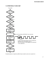
Page 97: ...n SWVDD H 137pin Source keys operative Completes power on operation After that proceed to each source operation SYSPW H 80pin Starts communication with Grille microcomputer Source ON 300ms 300ms In case of the above signal the communication with Grille microcomputer may fail If the time interval is not 300msec the oscillator may be defective ...

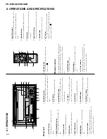
Page 98: ... on or off VOLUME button Press to increase or decrease the volume TAPE EJECT button Press to eject a tape from your cassette player ENT ENT DISP DISP CLOCK CLOCK LOUD LOUD SOURCE SOURCE OFF OFF 6 5 4 3 2 1 F D A 1 5 7 6 9 0 8 3 4 2 DETACH button Press to remove the front panel from the head unit Remote control The supplied remote control enables convenient remote operation of the head unit Operati...

Page 99: ...yer Sources off Notes In the following cases the sound source will not change When a product corresponding to each source is not connected to this unit When no disc is set in this unit When no cassette is set in this unit When no magazine is set in the multi CD player When the AUX external input is set to off External unit refers to a Pioneer product such as one available in the future that althou...

Page 100: ...until you see Tuner displayed 2 Use VOLUME to adjust the sound level When you press VOLUME up the volume is raised and when pressed down the volume is lowered 3 Press BAND ESC to select a band Press BAND ESC until the desired band is dis played F1 F2 F3 or AM 4 6 8 5 ENT ENT DISP DISP CLOCK CLOCK LOUD LOUD SOURCE SOURCE OFF OFF 6 5 4 3 2 1 F D A 7 5 6 4 1 3 2 4 To perform manual tuning press 2 or ...

Page 101: ...tape 2 After a cassette tape has been inserted press SOURCE OFF on the head unit or CAS SETTE on the remote to select the cassette player Press SOURCE OFF or CASSETTE until you see Cassette displayed 3 Use VOLUME to adjust the sound level When you press VOLUME up the volume is raised and when pressed down the volume is lowered 4 To perform fast forward or rewind press 2 or 3 FF or REW appears in t...

Page 102: ...ss SOURCE OFF or CD until you see CompactDisc displayed 4 5 7 ENT ENT DISP DISP CLOCK CLOCK LOUD LOUD SOURCE SOURCE OFF OFF 6 5 4 3 2 1 F D A 3 4 6 5 1 2 3 Use VOLUME to adjust the sound level When you press VOLUME up the volume is raised and when pressed down the volume is lowered 4 To perform fast forward or reverse press and hold 2 or 3 5 To skip back or forward to another track press 2 or 3 Pr...

Page 103: ...ti CD displayed 4 5 9 6 ENT ENT DISP DISP CLOCK CLOCK LOUD LOUD SOURCE SOURCE OFF OFF 6 5 4 3 2 1 F D A 8 4 5 6 7 1 2 3 2 Use VOLUME to adjust the sound level When you press VOLUME up the volume is raised and when pressed down the volume is lowered 3 Select a disc you want to listen to with the 1 to 6 buttons For discs located at 1 to 6 press the correspond ing number button If you want to select ...

Page 104: ...s that are not connected to speakers Yellow To terminal always supplied with power regardless of ignition switch position Orange white To lighting switch terminal Red To electric terminal controlled by ignition switch 12 V DC ON OFF Power amp sold separately Yellow black If you use a cellular telephone connect it via the Audio Mute lead on the cellular telephone If not keep the Audio Mute lead fre...

Page 105: ...tivity 18 µV S N 20 dB Selectivity 50 dB 10 kHz Note Specifications and the design are subject to possible modifications without notice due to improvements 8 2 SPECIFICATIONS FH P4000 X1N UC FH P4000R X1N EW Specifications General Power source 14 4 V DC 10 8 15 1 V allowable Grounding system Negative type Max current consumption 10 0 A Backup current 3 mA or less Dimensions W H D Chassis 178 100 1...

Page 106: ...c Signal format Sampling frequency 44 1 kHz Number of quantization bits 16 linear Frequency characteristics 5 20 000 Hz 1 dB Signal to noise ratio 94 dB 1 kHz IEC A network Dynamic range 92 dB 1 kHz Number of channels 2 stereo Cassette player Tape Compact cassette tape C 30 C 90 Tape speed 4 76 cm sec 0 14 cm sec 0 05 cm sec Fast forward rewinding time Approx 100 sec C 60 Wow flutter 0 09 WRMS Fre...

Reviews: