89
C-AX10
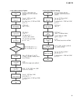
Mute ON
Input switch
Center DSP
setup
A/D
power down
Front DSP
coefficient transmission
fs check
Cancel the mute
DIR initialized
DIR lock ?
&
PLL lock ?
No
Yes
Receive a switching data from
the system control microcomputer
(IC2109).
IC1603-pin 9
Input "L" to RX.
IC1501
Transmit the program and coefficient
DIR : IC1603-pin 25 = "L" ?
PLL : IC1618-pin 15 = "H" ?
State of IC1603-pins 2, 3 and 27
(However, this state is between 50 ms
since DIR locks.)
IC1701, IC1702, IC1801 and IC1802
Transmit the coefficient
IC2118-pin 4
XADC = H
IC1405-pins 9 to 11
Control the SELA to SELC.
Front ch : IC1703 and IC1803
pins 42 and 43 = L
Excepting front ch : IC1902 and IC2002
pin 15 = H
IC1105, IC2704 and IC2804
pin 10 = L to H
Start
End
Mute ON
A/D
calibration
Center DSP
setup
Front DSP
coefficient transmission
Cancel the mute
Input switch
Receive a switching data from
the system control microcomputer
(IC2109).
IC1501
Transmit the program and coefficient
IC1701, IC1702, IC1801 and IC1802
Transmit the coefficient
IC2118-pin 4
XADC = L
Front ch : IC1703 and IC1803
pins 42 and 43 = H
Excepting front ch : IC1902 and IC2002
pin 15 = L
Front ch : IC1703 and IC1803
pins 42 and 43 = L
Excepting front ch : IC1902 and IC2002
pin 15 = H
Start
End
IC2118-pin 7
X24M = L (24MHz oscillation)
IC1105, IC2704 and IC2804
pin 10 = L to H
• Input switch (Analog to Digital)
• Input switch (Digital to Analog)
Front ch : IC1703 and IC1803
pins 42 and 43 = L
Excepting front ch : IC1902 and IC2002
pin 15 = H
Summary of Contents for C-AX10
Page 9: ...9 C AX10 ...
Page 13: ...C AX10 13 A B C D 1 2 3 4 1 2 3 4 E FRAD ASSY F CRAD ASSY 24 576MHz 24 576MHz 3 1 3 A D BLOCK ...
Page 14: ...C AX10 14 A B C D 1 2 3 4 1 2 3 4 H AUDIO A ASSY 3 1 4 D A BLOCK AUDIO A ASSY ...
Page 15: ...C AX10 15 A B C D 1 2 3 4 1 2 3 4 I AUDIO B ASSY 3 1 5 D A BLOCK AUDIO B ASSY ...
Page 16: ...C AX10 16 A B C D 1 2 3 4 1 2 3 4 A DIGITAL I O ASSY B DSP ASSY 3 1 6 DIGITAL SIGNAL BLOCK ...
Page 17: ...C AX10 17 A B C D 5 6 7 8 5 6 7 8 to D A SECTION Hi bit Hi bit Hi bit ...
Page 18: ...C AX10 18 A B C D 1 2 3 4 1 2 3 4 A E F Hi bit Hi bit Hi bit FRONT 3 1 7 µ COM PORT BLOCK ...
Page 35: ...C AX10 35 A B C D 5 6 7 8 5 6 7 8 AUDIO SIGNAL ROUTE 9 3 3V 3 3V x2 1 10W 3 6 G ...
Page 37: ...C AX10 37 A B C D 5 6 7 8 5 6 7 8 AUDIO SIGNAL ROUTE G1 6 11 11 4 6 G ...
Page 39: ...C AX10 39 A B C D 5 6 7 8 5 6 7 8 G1 6 5 6 G ...
Page 66: ...C AX10 66 A B C D 1 2 3 4 1 2 3 4 AUDIO A ASSY H SIDE B Q910 Q912 Q908 Q902 Q901 Q907 Q903 H ...
Page 67: ...C AX10 67 A B C D 5 6 7 8 5 6 7 8 Q901 Q905 Q906 Q904 907 Q903 ANP7291 D H ...
Page 71: ...C AX10 71 A B C D 5 6 7 8 5 6 7 8 Q1003 Q1007 Q1001 Q1005 Q1006 Q1004 Q1009 ANP7291 D I ...

