background image

Service Modes, Error Codes, and Fault Finding

EN 16

LC7.2E LA

5.

5.

Service Modes, Error Codes, and Fault Finding

Index of this chapter:

5.1  Test Points
5.2  Service Modes
5.3  Service Tools
5.4  Error Codes
5.5  The Blinking LED Procedure
5.6  Software Upgrading
5.7  Fault Finding and Repair Tips

5.1

Test Points

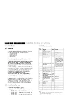
In the chassis schematics and layout overviews, the test points 
(Fxxx) are mentioned. In the schematics, test points are 
indicated with a rectangular box around “Fxxx” or “Ixxx”, in the 
layout overviews with a “half-moon” sign.
As most signals are digital, it will be difficult to measure 
waveforms with a standard oscilloscope. Several key ICs are 
capable of generating test patterns, which can be controlled via 
ComPair. In this way it is possible to determine which part is 
defective.
 
Perform measurements under the following conditions:

Service Default Mode.

Video: Colour bar signal.

Audio: 3 kHz left, 1 kHz right.

5.2

Service Modes

The Service Mode feature is split into four parts: 

Service Default Mode (SDM).

Service Alignment Mode (SAM).

Customer Service Mode (CSM) and Digital Customer 
Service Mode (DCSM).

Computer Aided Repair Mode (ComPair).

 
SDM and SAM offer features, which can be used by the Service 
engineer to repair/align a TV set. Some features are: 

A pre-defined situation to ensure measurements can be 
made under uniform conditions (SDM).

Activates the blinking LED procedure for error identification 
when no picture is available (SDM).

The possibility to overrule software protections when SDM 
was entered via the Service pins.

Make alignments (e.g. white tone), (de)select options, 
enter options codes, reset the error buffer (SAM).

Display information (“SDM” or “SAM” indication in upper 
right corner of screen, error buffer, software version, 
operating hours, options and option codes, sub menus).

 
The (D)CSM is a Service Mode that can be enabled by the 
consumer. The CSM displays diagnosis information, which the 
customer can forward to the dealer or call centre. In CSM 
mode, “CSM”, is displayed in the top right corner of the screen. 
The information provided in CSM and the purpose of CSM is to:

Increase the home repair hit rate.

Decrease the number of nuisance calls.

Solved customers' problem without home visit.

 
ComPair Mode is used for communication between a computer 
and a TV on I2C /UART level and can be used by a Service 
engineer to quickly diagnose the TV set by reading out error 
codes, read and write in NVMs, communicate with ICs and the 
uP (PWM, registers, etc.), and by making use of a fault finding 
database. It will also be possible to up and download the 
software of the TV set via I2C with help of ComPair. To do this, 
ComPair has to be connected to the TV set via the ComPair 
connector, which will be accessible through the rear of the set 
(without removing the rear cover).

5.2.1

General

Some items are applicable to all Service Modes or are general. 
These are listed below.

Life Timer

During the life time cycle of the TV set, a timer is kept. It counts 
the normal operation hours (not the Stand-by hours). The 
actual value of the timer is displayed in SDM and CSM in a 
decimal value. Every two soft-resets increase the hour by +1.

Software Identification, Version, and Cluster

The software ID, version, and cluster will be shown in the main 
menu display of SDM, SAM, and CSM.
The screen will show: “

AAAABCD X.YY

”, where: 

AAAA

 is the chassis name: LC71 for analogue range (non-

DVB), LC72 for digital range (DVB).

B

 is the region indication: E= Europe, A= AP/China, U= 

NAFTA, L= LATAM.

C

 is the display indication: L= LCD, P= Plasma.

D

 is the language/feature indication: 1= standard, H= 

1080p full HD.

X

 is the main version number: this is updated with a major 

change of specification (incompatible with the previous 
software version). Numbering will go from 1 - 9 and A - Z.

If the main version number changes, the new version 
number is written in the NVM.

If the main version number changes, the default 
settings are loaded.

YY

 is the sub version number: this is updated with a minor 

change (backwards compatible with the previous versions) 
Numbering will go from 00 - 99.

If the sub version number changes, the new version 
number is written in the NVM.

If the NVM is fresh, the software identification, version, 
and cluster will be written to NVM.

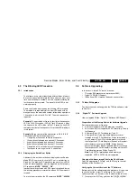
Display Option Code Selection

When after an SSB or display exchange, the display option 
code is not set properly, it will result in a TV with “no display”. 
Therefore, 

it is required

 to set this display option code after 

such a repair.
To do so, press the following key sequence on a standard RC 
transmitter: “

062598

” directly followed by 

MENU

 and “

xxx

”, 

where “xxx” is a 3 digit decimal value of the panel type: see 
column “Panel Code” in table “Option Codes OP1...OP7” (ch. 
8), or see sticker on the side/bottom of the cabinet. When the 
value is accepted and stored in NVM, the set will switch to 
Stand-by, to indicate that the process has been completed.

Figure 5-1 Location of Display Option Code sticker

During this algorithm, the NVM-content must be filtered, 
because several items in the NVM are TV-related and not SSB-
related (e.g. Model and Prod. S/N). Therefore, “Model” and 
“Prod. S/N” data is changed into “See Type Plate”.
In case a call centre or consumer reads “See Type Plate” in 
CSM mode, he needs to look to the side/bottom sticker to 
identify the set, for further actions.

PHILIPS

MODEL:

32PF9968/10

PROD.SERIAL NO:

AG 1A0620 000001

040

39mm

27mm

(CTN Sticker)

Display Option

Code

E_06532_038.eps

290107

Summary of Contents for LC7.2E

Page 1: ...ing Diagram 37 42 ME7 Promo Set 31 Wiring Diagram 42 1080p 32 Wiring Diagram 47 ME7 33 Wiring Diagram 47 1080p ME7 34 Block Diagram Video 35 SSB Headphone Amp Muting B06D 54 57 66 SSB Audio B07 55 57 66 SSB SRP List 56 57 66 Side A V Panel D 67 68 Keyboard Control Panel E 69 70 1080P Panel On Chip uController F1 71 78 1080P Panel Flash NVM F2 72 78 1080P Panel LVDS In F3 73 78 1080P Panel LVDS Out...

Page 2: ...n contrast ratio 3500 1 26 4000 1 32 5000 1 37 5000 1 42 Min light output cd m2 500 Typ response time ms 8 26 32 6 37 5 42 Viewing angle HxV degrees 160x150 26 176x176 26 Tuning system PLL Presets channels 100 presets Tuner bands VHF UHF S H TV Colour systems PAL B G D K I SECAM B G D K L L DVB T COFDM Video playback NTSC PAL SECAM 1 1 3 Miscellaneous Power supply Mains voltage VAC 220 240 Mains f...

Page 3: ...Head phone Out Bk Head phone 32 600 ohm 10 mW rt EXT3 Cinch Video CVBS In Audio In Rd Audio R 0 5 VRMS 10 kohm jq Wh Audio L 0 5 VRMS 10 kohm jq Ye Video CVBS 1 VPP 75 ohm jq 8 Function Select 0 2 V INT 4 5 7 V EXT 16 9 9 5 12 V EXT 4 3 j 9 Ground Green Gnd H 10 Easylink P50 0 5 V 4 7 kohm jk 11 Video Green 0 7 VPP 75 ohm j 12 n c 13 Ground Red Gnd H 14 Ground P50 Gnd H 15 Video Red 0 7 VPP 75 ohm...

Page 4: ...annel j 2 Shield Gnd H 3 D2 Data channel j 4 D1 Data channel j 5 Shield Gnd H 6 D1 Data channel j 7 D0 Data channel j 8 Shield Gnd H 9 D0 Data channel j 10 CLK Data channel j 11 Shield Gnd H 12 CLK Data channel j 13 n c 14 n c 15 DDC_SCL DDC clock j 16 DDC_SDA DDC data jk 17 Ground Gnd H 18 5V j 19 HPD Hot Plug Detect j 20 Ground Gnd H EXT4 Cinch Video YPbPr In Audio In Gn Video Y 1 VPP 75 ohm jq ...

Page 5: ... Overview EN 5 LC7 2E LA 1 Figure 1 5 PWB CBA locations 37 and 42 models without 1080p module H_16940_008 eps 050307 B POWER SUPPLY UNIT D SIDE I O PANEL SMALL SIGNAL BOARD J LED PANEL E CONTROL PANEL POWER SUPPLY UNIT D SIDE I O PANEL F 1080p PANEL ...

Page 6: ... the two pins of the Mains AC Power plug Check the cabinet for defects to prevent touching of any inner parts by the customer Service Default Mode see chapter 5 with a colour bar signal and stereo sound L 3 kHz R 1 kHz unless stated otherwise and picture carrier at 475 25 MHz for PAL or 61 25 MHz for NTSC channel 3 Where necessary measure the waveforms and voltages with D and without E aerial sign...

Page 7: ...entification The bottom line of a type plate gives a 14 digit serial number Digits 1 and 2 refer to the production centre e g AG is Bruges digit 3 refers to the B O M code digit 4 refers to the Service version change code digits 5 and 6 refer to the production year and digits 7 and 8 refer to production week in example below it is 2006 week 17 The 6 last digits contain the serial number Figure 2 1...

Page 8: ...apter 4 1 Cable Dressing 4 2 Service Positions 4 3 Assy Panel Removal 4 4 Set Re assembly Notes Figures below can deviate slightly from the actual situation due to the different set executions Follow the disassemble instructions in described order 4 1 Cable Dressing LC07 26 BASIC SET ...

Page 9: ...Mechanical Instructions EN 9 LC7 2E LA 4 Figure 4 2 Cable dressing 32 inch models G_16860_064 eps 310107 ...

Page 10: ...Mechanical Instructions EN 10 LC7 2E LA 4 Figure 4 4 Cable dressing 42 models without 1080p module H_16940_009 eps 050307 ...

Page 11: ...sure that the foam bars are always supporting the cabinet and never only the display Caution Failure to follow these guidelines can seriously damage the display By laying the TV face down on the ESD protective foam bars 4 3 Assy Panel Removal 4 3 1 Rear Cover Warning Disconnect the mains power cord before you remove the rear cover 1 Place the TV set upside down on a table top using the foam bars s...

Page 12: ...3 3 4 3 4 IR LED Panel 1 Refer to next figure is taken from the 32 model but the method is comparable for the other screen sizes 2 Unplug connector s 1 3 Release clip 2 and remove the board When defective replace the whole unit G_16860_066 eps 010207 a b 1x b 1x c G_16860_077 eps 010207 2 g f 1 2 ...

Page 13: ...figure 2 Unplug connectors 1 3 Remove screws 2 Figure 4 15 Tweeters 4 3 6 1080p Panel 1 Refer to next figure s 2 Unplug cables a Be careful with the LVDS connectors as they are very fragile 3 Remove the fixation screws b 4 Take the board out it hinges at the lower side 5 Remove the screws c that fixate the top and bottom shieldings and remove the shieldings Note Pay special attention not to damage...

Page 14: ...cribed below 1 Refer to next figure is taken from the 32 model but the method is comparable for the other screen sizes 2 Unplug cables a 3 Remove the fixation screws b 4 Take the board out it hinges at the left side Figure 4 19 Main supply panel 32 model 4 3 8 Small Signal Board SSB 1 Refer to next figure is taken from the 32 model but the method is comparable for the other screen sizes G_16860_06...

Page 15: ...he LED IR board c 3 Unplug the connectors d from the loudspeakers 4 Do NOT forget to unplug the LVDS connector e from the SSB Important Be careful as this is a fragile connector 5 Remove T10 parker screw b that holds the Side I O module bracket 6 Remove T10 parker screws f of the central sub frame 7 Remove LCD panel fixation screws g and lift the complete central sub frame from the set incl the PS...

Page 16: ... items are applicable to all Service Modes or are general These are listed below Life Timer During the life time cycle of the TV set a timer is kept It counts the normal operation hours not the Stand by hours The actual value of the timer is displayed in SDM and CSM in a decimal value Every two soft resets increase the hour by 1 Software Identification Version and Cluster The software ID version a...

Page 17: ...icate that the television is in Service Default Mode Figure 5 3 SDM menu Menu explanation HHHHH Are the operating hours in decimal AAAABCD X YY See paragraph Service Modes General Software Identification Version and Cluster for the SW name definition SDM The character SDM to indicate that the TV set is in Service mode ERR Shows all errors detected since the last time the buffer was erased Five err...

Page 18: ...rol transmitter The selected item will be indicated When not all menu items fit on the screen use the MENU UP DOWN keys to display the next previous menu items With the MENU LEFT RIGHT keys it is possible to Activate the selected menu item Change the value of the selected menu item Activate the selected sub menu When you press the MENU button twice while in top level SAM the set will switch to the...

Page 19: ...b set of the main SW 9 LIFE TIMER Operating hours indication 10 TUNER Indicates the tuner signal condition Weak when signal falls below threshold value Medium when signal is at mid range and Strong when signal falls above threshold value 11 SYSTEM Gives information about the video system of the selected transmitter PAL SECAM NTSC 12 SOUND Gives information about the audio system of the selected tr...

Page 20: ... entries while keying this sequence Then the Service menu will appear see figures below Alternative method to activate DCSM press key sequence 123654 on the remote control transmitter while in digital mode do not allow the display to time out between entries while keying the sequence Then the Service menu will appear see figures below Menu explanation Figure 5 8 DCSM menu 3 1 Hardware version This...

Page 21: ...lled ComPair Assistant 1 may help you to identify in case the TV does not show any picture whether the Small Signal Board SSB or the display of a Flat TV is defective Thus to determine if LVDS RGB and sync signals are okay When operating the tool will show a small scaled picture on a VGA monitor Due to a limited memory capacity it is not possible to increase the size when processing high resolutio...

Page 22: ...r buffer TV s NVM except when the NVM itself is defective 5 4 2 How to Read the Error Buffer You can read the error buffer in 3 ways On screen via the SAM SDM CSM if you have a picture Example ERROR 0 0 0 0 0 No errors detected ERROR 6 0 0 0 0 Error code 6 is the last and only detected error ERROR 9 6 0 0 0 Error code 6 was detected first and Table 5 3 Error code overview Notes 1 Some of the error...

Page 23: ...following RC sequence MUTE 062500 OK In order to avoid confusion with RC5 signal reception blinking this blinking procedure is terminated when a RC5 command is received To erase the error buffer the RC command MUTE 062599 5 6 Software Upgrading In this chassis three SW stacks are used TV mains SW processor and processor NVM Digital TV SW IBO Zapper 1080p Panel SW if present depends on execution 5 ...

Page 24: ...grade procedure In case of a power drop during the upgrade procedure don t remove the portable memory from the TV The TV will continue the upgrade as soon as the power comes back Example At start up of the TV the current software is erased Figure 5 11 Erasure of the software If the erasure is successful the programming will start Figure 5 14 Upgrade ready When the software upgrade has been success...

Page 25: ...n the SSB keep short Alternative method 1 1 Go to SAM 2 Select NVM Editor 3 Select ADR address to 1 dec 4 Change the VAL value to 170 dec 5 Store the value 6 Do a hard reset to make sure new default values took place Alternative method 2 It is also possible to upload the default values to the NVM with ComPair in case the SW is changed the NVM is replaced with a new empty one or when the NVM conten...

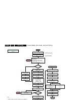
Page 26: ...00ms Time out 2000ms No Error 2 Protection Wait for 100ms Blank Picture Picture Mode Setup Detection Yes LED BLUE for Normal mode LED RED for Recording mode User wake up the sets in DVB recording mode BLOCK RC Key Yes Standby Normal Mode RED LED 1000ms to 1500ms 500ms 100ms Notes 1 LC07 TV software only start communication with IBOZ once 160ms Port Assignment in STANDBY unBlank Picture UnMute Audi...

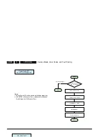
Page 27: ...A 5 SEMISTANDBY STANDBY Start Mute Audio Software Shutdown BL_ON_OFF LOW Wait 300ms Switch OFF LVDS Wait 20ms LCD_PWR_ON LOW Standby using power key LED RED No Yes For DVB Sets only Semistandby BL_ADJ stop dimming PWM duty cycle 100 300ms 20ms Wait for 3000ms ...

Page 28: ...ower Down INT AC OFF or Transient INT DC_PROT INT STANDBYn LOW Wait 5000 ms Re start Start up End No Notes 1 Power Down INT will be based on fall edge triggering 2 3V3STBY will stay for 15ms software must perform WriteProtect for NVM within 15ms Poll the Power Down INT for 5 times End Avoid false trigger Yes ...

Page 29: ...D SIDE I O J IR LED LIGHT SENSOR 8304 8M20 8C01 8735 8735 8521 8520 8002 CN6 9P 1M01 3P 8M01 LVDS 30P 1P11 8P 8P11 8G51 MAIN SUPPLY INVERTER 8191 8192 UK 1005 1116 1114 1112 LCD DISPLAY 1004 ONLY USED FOR LPL PANEL 5200 5200 TUNER CN2 DISPLAY SUPPLY 1 24V 2 24V 3 24V 4 24V 5 24V 6 GND 7 GND 8 GND 9 GND 10 GND 11 DIM 12 BL ON 13 PWM 14 N C CN3 DISPLAY SUPPLY 1 24V 2 24V 3 24V 4 24V 5 24V 6 GND 7 GN...

Page 30: ...101 2P3 INLET X403 12P X404 14P WIRING 37 42 LCD STYLING ME7 CN2 14P CN3 12P G_16860_094 eps 180707 RIGHT SPEAKER LEFT SPEAKER B SSB E KEYBOARD CONTROL D SIDE I O J IR LED LIGHT SENSOR 8304 8M20 8735 8521 8520 8002 1M01 3P 8M01 LVDS 30P 1P11 8P 8G51 MAIN SUPPLY INVERTER INVERTER X406 8P X412 9P 8C01 8P11 8191 8192 UK 1005 1116 1114 1112 LCD DISPLAY 1004 ...

Page 31: ... D SIDE I O J IR LED LIGHT SENSOR 8304 8M20 8735 8002 1M01 3P 8M01 LVDS 30P 1P11 8P 8G51 MAIN SUPPLY INTEGRATED POWER BOARD PANEL HV CONNECTOR CN207 2P 8C01 8P11 8191 8192 UK 1005 1116 1114 1112 LCD DISPLAY 1004 CN202 8P CN201 9P CN206 2P PANEL HV CONNECTOR High Voltage HV Cable to panel 2x is provided by supplier on PSU for Delta s Integrated power Board IPB CN201 1 12Va 2 12Va 3 GND 4 5 2Vs 5 5 ...

Page 32: ...80p STYLING ME7 CN2 14P CN3 12P G_16860_095 eps 190707 RIGHT SPEAKER LEFT SPEAKER B SSB E KEYBOARD CONTROL D SIDE I O J IR LED LIGHT SENSOR 8304 8M20 8735 8521 8520 8002 1M01 3P 8M01 LVDS 51P 1P11 8P 8G51 MAIN SUPPLY INVERTER INVERTER X406 8P X412 9P 8C01 8P11 8191 8192 UK 1005 1116 1114 1112 LCD DISPLAY 1004 1G51 40P 1G52 41P 1710 4P X405 4P F 1080p BOLT ON 8G52 8710 5201 5201 TUNER ONLY USED FOR...

Page 33: ...2 1M01 3P 8M01 LVDS 30P 1P11 8P 8G51 MAIN SUPPLY INVERTER INVERTER CN3 12P CN2 14P 8C01 8P11 8191 8192 UK 1005 1116 1114 1112 LCD DISPLAY 1004 CN6 9P CN7 8P CN2 1 24Vinv 2 24Vinv 3 24Vinv 4 24Vinv 5 24Vinv 6 GND3 7 GND3 8 GND3 9 GND3 10 GND3 11 Vbri 12 ON PFF 13 PWM 14 GND CN3 1 24Vinv 2 24Vinv 3 24Vinv 4 24Vinv 5 24Vinv 6 GND3 7 GND3 8 GND3 9 GND3 10 GND3 11 N C 12 N C CN6 1 12V Audio 2 12V Audio...

Page 34: ...N SUPPLY INVERTER INVERTER CN3 12P CN2 14P 8C01 8P11 8191 8192 UK 1005 1116 1114 1112 LCD DISPLAY 1004 CN6 9P CN7 8P CN2 1 24Vinv 2 24Vinv 3 24Vinv 4 24Vinv 5 24Vinv 6 GND3 7 GND3 8 GND3 9 GND3 10 GND3 11 Vbri 12 ON PFF 13 PWM 14 GND CN3 1 24Vinv 2 24Vinv 3 24Vinv 4 24Vinv 5 24Vinv 6 GND3 7 GND3 8 GND3 9 GND3 10 GND3 11 N C 12 N C CN6 1 12V Audio 2 12V Audio 3 GND2 Audio 4 5V2stby 5 5V2stby 6 5V2s...

Page 35: ... 1211 TXAn 51 50 49 48 45 44 43 42 41 40 BOLT_ON_SCL BOLT_ON_SDA TXCn1 TXCp1 TXCLKn1 TXCLKp1 TXDn1 TXDp1 TXAp1 TXBn1 TXBp1 TXAn1 TA1 TB1 TC1 TCLK1 TD1 VDISP SC1_RF_OUT_CVBS PR_R2 162 190 PR_R3 FS2 CVBS_OUT2 70 Y_G1 PB_B3 PR_R1 Y_G3 C RF_AGC 12 13 7111 14 RF_AGC_IBO B03B 169 CVBS1 MEMORY 8 BIT SINGLE LVDS TX DIN_PORTD 24BIT SOUND TRAPS 4 5 to 6 5 Mhz VIF PLL SINGLE REFERENCE QSS MIXER INTERCARRIER ...

Page 36: ...IO LS_R 7A01 TDA8932T N1 CLASS D POWER AMPLIFIER 9 1 27 22 ENGAGE 5 1 2 RIGHT SPEAKER HDMI_I2S_SCK 1 86 HDNI_I2S_WS 2 85 HDMI_I2S_SD 3 84 8 77 BCK WS DATAI MUTE SCK WS SD0 MUTE AUDIO DAC 1735 3 4 LEFT SPEAKER DC DETECTION STANDBYn 6 3A19 3A03 3A11 7901 HP_AUDIO_OUT_L HP_AUDIO_OUT_R HP_LOUT HP_ROUT MUTING ANTI_PLOP 19 1 18 2 RXxxB 14 16 VOUTL VOUTR SC1_AUDIO _MUTE_R SC1_AUDIO _MUTE_L SC2_AUDIO _MUT...

Page 37: ...16x4 DQ 0 31 CX_MA 0 11 R0 HDMI_Cb 0 7 HDMI_Y 0 7 HDMI_Cr 0 7 19 1 18 2 2x HDMI CONNECTOR RXxxA 19 1 18 2 RXxxB 7817 SII9025CTU R1 SDRAM_CLK 38 136 A_MICLK 20 110 A_MOCLK 57 118 TS_CLK 63 29 GPIO RESET_STV 34 32 TDA_CLK 37 50 37 38 37 38 112 111 CX_MCLK CX_CLKE HDMI_CCLK 121 23 1101 TD1316AF IHP 2 MAIN TUNER HYBRID 6 4MHZ_CLK 54 1 4MHZ_MOJO 158 1 7F03 7F02 TXCLKn 43 TXCLKn1 20 TXCLKP 42 TXCLKP1 TO...

Page 38: ...FK49 E8 FK50 D8 FK51 E8 FK52 E8 FK53 E8 FK54 D8 FK55 E8 FK56 E8 FK57 E8 FK58 D8 FK59 E8 FK60 E8 FK61 E8 FK62 E10 FK63 E8 FK67 E10 FK68 E10 FK69 E10 FK70 D10 FK71 E10 FK72 E10 FK73 E9 FK74 D9 FK75 E9 FK80 D10 FK81 F10 FK82 F9 FK83 D9 FK84 F9 FL20 A2 FL21 A2 FL22 A2 FL23 A2 FL24 A2 FL25 A2 FL26 A2 I110 E5 I111 E7 I112 E5 I114 E5 I118 E5 I120 E5 I121 E7 I122 F6 I123 E6 I124 D5 I125 D5 I126 D5 I127 D5...

Page 39: ... TDA9886T V4 DEMODULATOR 3129 3128 ERR 08 7111 74HCT4053D 1 3 2 5 I2C_TDA_SDA I2C_TDA_SCL 8 6 7F01 TDA10046AHT COFDM CHANNEL DECODER 3F40 3F44 5V_SW 3F41 3F42 9 8 7G00 PNX8314HS MOJO 3G47 3G46 ERR 12 I2C_LOCAL_SDA I2C_LOCAL_SCL 7 6 30 31 7K00 STV0700L PCMCIA CONTROLLER 3K01 3K00 5 6 7H03 M24C64 EEPROM 8Kx8 3H09 3H10 5V_SW 3H12 3H13 5 6 7315 M24C64 EEPROM NVM 3357 3355 ERR 06 7320 7321 3V3_SW 3308 ...

Page 40: ... 5219 VDISP 12V_DISP 12V_DISP 7210 B02 5215 7208 CONTROL 5217 5V_SW 5V_SW B02 5VHDMI_A 18 HDMI CONNECTOR 1 5VHDMI_B 1811 18 HDMI CONNECTOR 2 1810 5V_SW 5V_SW 3V3_STBY 3V3_STBY B02 B02 AUDIO_POWER AUDIO_POWER AUDIO_POWER_ 12V_DISP B02 4A01 RES VDDA VDD 5A05 3A01 AUDIO_POWER AUDIO_POWER B02 VSSA VSS 5A06 3A02 B04a B06d B03a f B04a b B06c B03f B03d B03a B03b B04b CN7 X412 CN01 CN6 X406 CN02 3L10 1M20...

Page 41: ...6 FC25 2C56 1n0 1n0 2C57 2C55 1n0 AUDIO_POWER AUDIO_POWER GNDSND 7 8 12V_DISP 5V_STANDBY 1 2 3 4 5 6 8 9 B8B PH K S 1P11 1 2 3 4 5 6 7 1C01 B9B PH K 2B19 22u 35V 1B11 1 2 3 4 5 B3B PH SM4 TBT LF 6K8 3B18 FB14 IB15 3B10 IB14 GNDTUN 2B20 100p 1K0 3B15 6B02 BZX384 C33 VTUN 6B03 BAV99 5B04 100u 7B03 2N7002 220R 3B13 2B16 10n 2B11 100n 2B25 4B01 3B11 4K7 10u 5B02 5B03 33u 100n 2B17 16V 470u 2B13 IB17 F...

Page 42: ...I114 C4 I118 C4 I120 D2 I121 D10 I122 D7 I123 E10 I124 E3 I125 F4 I126 F3 I127 F3 I128 G6 I129 G6 I130 H6 I131 H5 I133 I4 I135 I4 I136 I4 I137 B8 I138 G7 I139 G7 I141 D1 I142 F5 I143 H3 I144 H4 I145 A9 I146 A8 I147 A8 I131 7109 BC847B 4125 5121 120R 5120 120R I147 I146 2149 2u2 50V 10u 2151 I145 5118 220R 12V_DISP 100n 2148 330n 2147 47R 3137 3 47R 3136 7133 L78M05CDT 2 1 1u0 2146 3135 15R I143 I1...

Page 43: ...IF28 33R 2 7 1 8 3F34 2 1 8 33R 3F34 1 33R 3F32 1 33R 2 7 33R 3F32 3 3 6 3F32 2 3F32 4 4 5 1 8 33R 2 7 3F31 1 33R 3F31 2 33R 33R 3F31 3 3 6 33R 4 5 10p 2F33 3F31 4 100n 2F30 4K7 3F23 IF31 4F11 100n 2F27 3F24 100K 5 6 7 8 4 4 LM393D 7F04 2 LM393D 7F04 1 3 2 1 8 60R 5F11 IF26 IF27 IF25 IF24 IF22 IF23 IF21 FF28 IF20 FF26 FF22 IF10 IF13 IF16 IF15 4F12 IF14 1K0 4K7 3F20 100n 3F26 2F29 3F48 100R 100R 3F...

Page 44: ...FK42 FK43 FK45 FK44 FK46 FK47 FK49 FK48 FK50 FK51 FK53 FK52 FK54 FK55 FK57 FK56 FK58 FK59 FK61 IK68 FK60 IK69 IK73 IK75 IK76 FK84 FK06 IK72 IK70 1 4 VDD 3 5V_SW 27M 7K04 OC GND 2 33R 3K05 4 3K12 10K 3K05 3 33R 33R 3K05 2 3K05 1 33R 3K03 4 3K03 3 33R 33R 33R 3K03 2 3K03 1 33R 33R 3K02 3 33R 3K02 1 3K02 2 33R 100n 2K03 100n 2K05 2K02 100n 5K01 PCMCIA_AVCC PCMCIA_VPP 60R 5K02 60R PCMCIA_5V 5 SET 10K ...

Page 45: ...G17 16V 10u FG27 FG28 FG25 FG24 FG35 FG36 FG34 FG32 FG18 FG39 FG37 3V3 3V3 3G65 1K0 1 33n 2G34 NCP303LSN30 7G06 CD 5 GND 3 INP 2 4 NC OUTP 3 4 1 2 3V3 3V3 SKQTLB 1G03 3V3 3V3 10K FG29 3G54 3G55 10K 10K 3G51 FG30 3G37 10K 3G36 10K 10K 3G31 3G28 3V3 3G29 10K 10K 10K 3G30 3G63 10K 3G62 3G61 33R 3G60 33R 4 5 33R 7 3G59 4 33R 3G59 2 2 3G56 4 4 5 33R 3G56 2 2 7 33R 3G58 4 4 5 33R 4 5 33R 7 33R 3G57 4 3G...

Page 46: ...41 1 48 17 16 9 23 10 22 21 20 19 4Mx8 2Mx16 25 24 6 5 4 3 2 EPROM M29W320ET70N 7H00 FH00 4H12 3H09 100R 8 4 7 100R 3H10 M24C64 WMN6 7H03 1 2 3 6 5 8Kx8 Φ EEPROM 5H03 4H02 4H03 4H05 FH06 IH06 4H15 10K 3H05 2H04 100n FH07 43 49 28 41 54 6 12 46 52 16 15 36 40 18 39 1 14 27 3 9 50 51 53 5 7 8 10 11 13 42 44 20 21 17 37 38 19 2 4 45 47 48 22 35 25 26 29 30 31 32 33 34 EDS1216AGTA SYNC Φ 4x2Mx16 SDRAM...

Page 47: ...FJ24 D8 FJ25 D8 FJ26 D4 FJ27 E4 IJ01 B7 IJ02 B8 IJ11 A8 IJ63 B1 IJ64 C1 IJ65 C1 IJ66 C1 IJ67 D8 IJ68 D8 FJ22 PESD5V0S1BA 6J63 6J62 PESD5V0S1BA PESD5V0S1BA 6J61 6J60 PESD5V0S1BA BAS316 6J03 3J03 100R IJ68 IJ67 2J06 100n FJ23 IJ11 FJ02 FJ01 IJ02 IJ01 1002 1001 4J14 4J15 FJ25 FJ24 330p 330p 2J14 100R 3J15 2J15 3J14 100R 6J15 BZX384 C6V8 3 4 5 BZX384 C6V8 6J14 1J14 S3B PH SM4 TB 1 2 2J01 10u 16V 60R 5...

Page 48: ...4315 1R0 3L10 4313 F361 F362 F386 100R 100R 3L09 3L08 5 4308 1311 1 2 3 4 10K 3L07 3V3_STBY 10K 3L06 3L05 100R 6318 PDZ6 2 B 12V_DISP 220n 2338 3L04 1K5 7308 BC847BW 3V3_STBY BZX384 C3V3 6317 F309 3V3_STBY 100R 3L02 3L01 1K2 3300 4K7 3V3_STBY 3397 47K 3396 5V_STANDBY 1K0 PDTC114ET 7322 3V3_SW 3V3_SW 4306 4307 3K3 3308 3305 3K3 3374 3309 3 1 2 7320 3 1 2 7321 BSH111 3V3_SW BSH111 3V3_STBY 3V3_SW 3V...

Page 49: ...37 38 19 2 4 45 47 48 50 51 53 25 26 29 30 31 32 33 34 20 21 17 1M X 16 X 4 23 24 22 35 41 54 6 12 46 52 16 7205 IS42S16400D 6TL Φ DRAM 18 1 14 27 3 9 43 49 28 7 8 10 11 13 42 44 39 15 36 40 19 2 4 45 47 48 50 51 53 5 29 30 31 32 33 34 20 21 17 37 38 7204 IS42S16400D 6TL Φ 23 24 22 35 25 26 13 7 14 12 DRAM 1M X 16 X 4 10 74LCX14T 7211 6 74LCX14T 11 7 14 5V_SW 7211 5 5V_SW 3257 4K7 3V3_SW 4K7 3258 ...

Page 50: ...2443 1n5 1n5 2441 100n 2445 2440 470n 470n 2439 3420 100R 100R 3419 3418 100R 100R 3417 1R0 4402 3402 4401 12V_DISP I425 I417 I416 I418 I419 I414 I415 I413 I412 2424 10u 10u 2425 10u 2426 10u 2427 58 76 80 66 69 35 25 56 67 68 53 34 33 50 51 42 41 48 49 57 47 71 72 73 74 19 54 55 37 36 52 8 9 11 5 18 1 75 22 32 46 2 3 4 17 7 16 20 21 6 10 27 26 31 30 29 78 77 14 15 12 13 59 60 61 62 38 40 24 23 28...

Page 51: ...C3 1610 C7 1 2 3 4 5 6 7 8 9 10 11 1 2 3 4 5 6 3625 100R PESD5V0S1BA 6615 4604 4603 MSD 242V 01 NIDIP 765A LF 3 1 2 I636 1603 I635 3616 33K 33K 3615 3612 33K 33K 3608 150R 3611 150R 3607 150R 3621 9 150R 3620 6 GND 1601 3 1601 1 1 2 3 4 5 8 7 1601 2 I633 3619 100R 3618 100R 3617 100R F615 F616 F613 F614 F612 I611 I610 F606 F607 F605 F609 F610 F608 F611 6606 PESD5V0S1BA PESD5V0S1BA 6604 5V_SW 5V_SW...

Page 52: ...PESD5V0S1BA 6517 PESD5V0S1BA 6516 PESD5V0S1BA 6515 PESD5V0S1BA PESD5V0S1BA 6514 4504 BC857BW 7504 4502 BC857BW 7502 3540 4K7 4K7 3538 I556 I557 3555 68R I553 I554 I552 I551 1N4148 6513 1N4148 6512 220n 2534 2536 220n 3 4 5 6 7 8 9 12 13 14 15 16 17 18 19 2 20 21 PPTV 55 1506 1 10 11 21 3 4 5 6 7 8 9 13 14 15 16 17 18 19 2 20 1504 PPTV 55 1 10 11 12 33K 3515 3511 33K 33K 3513 3508 33K 3512 150R 350...

Page 53: ...4 33R 33R 3855 1 1 33R 2 7 33R 3 6 3855 2 33R 4 5 3855 3 3855 4 8 33R 3835 33R 3854 1 1 3854 2 2 7 33R 3 6 33R 4 5 3854 3 1 8 33R 3854 4 2 7 33R 3853 1 33R 3853 2 3853 3 33R 3 6 33R 3853 4 4 5 1 8 2 7 33R 3851 1 3 6 33R 3851 2 8 33R 3851 3 33R 1 3852 2 33R 2 7 3852 1 3852 3 3 6 33R 4 5 33R 4 5 3852 4 3851 4 33R F877 F876 F875 I822 I823 I820 I821 I856 I857 I855 I853 I854 I858 I852 I850 I851 F874 F8...

Page 54: ...0n 1 2 3 4 5 F903 1901 F902 2 1 3 YKB21 5157N 1900 470n 2907 3911 10K 7916 BC847BW 1 3 2 7913 BC847BW 1 3 2 7911 BC847BW 1 3 2 3 2 7912 BC847BW 1 3909 33R 3903 33R 2905 2901 33p 33p 3910 33R 33R 3904 I901 F910 F908 2908 220n 4 5V_SW 7901 1 TS482IDT 3 2 1 8 6 7 8 4 7901 2 TS482IDT 5 F904 F901 I905 I904 I902 I903 3907 100K 3902 120K 3905 47K 3901 47K 3906 100K 470n 120K 3908 2902 2904 470n 16V 100u ...

Page 55: ...2A13 D8 2A14 D8 2A15 D3 2A16 D3 1 2 3 4 5 6 7 8 9 10 11 1 2 3 4 5 6 7 8 9 5A04 22u 2A17 D8 2A18 D6 2A19 D4 2A20 E3 2A21 D7 2A22 E3 2A23 E8 2A24 E3 2A25 E6 2A26 E8 22u IA41 5A03 GNDSND 47n 2A47 2A46 47n AUDIO_POWER 60R 5A07 AUDIO_POWER_ 12V_DISP IA40 4A02 4A01 VSS VSSA VSSA GNDSND IA39 IA38 IA37 IA36 IA35 IA34 IA33 470n 2A28 470n 2A14 2A45 1n0 FA32 IA31 IA29 IA30 220u 2A04 220u 25V 25V GNDSND 2A08 ...

Page 56: ...03E 1x MIU_RDY B03C 1x MIU_RDY B03D 1x MIU_WEN B03C 1x MIU_WEN B03D 1x MIU_WEN B03E 1x MOJO_I2S_OUT_SCK B03D 1x MOJO_I2S_OUT_SCK B04C 1x MOJO_I2S_OUT_SD B03D 1x MOJO_I2S_OUT_SD B04C 1x MOJO_I2S_OUT_WS B03D 1x MOJO_I2S_OUT_WS B04C 1x MUTEn B04A 1x MUTEn B06D 1x NOR_CS B03D 1x NOR_CS B03E 1x NOR_RYBY B03D 1x NOR_RYBY B03E 1x NOR_WP B03D 1x NOR_WP B03E 1x PCMCIA_5V B03C 4x PCMCIA_AVCC B03C 3x PCMCIA_...

Page 57: ...9 2L33 A9 3113 E6 3116 E6 3117 E6 3118 E6 3119 E6 3122 E6 3125 D6 3126 D6 3130 D5 3133 D6 3135 D6 3201 B7 3202 B7 3203 B7 3204 B7 3212 B7 3213 A6 3215 B7 3216 A6 3223 A7 3224 A7 3225 A7 3226 A7 3227 A7 3229 D7 3231 D7 3232 D7 3233 A8 3235 A8 3238 A8 3239 D6 3240 D7 3246 A7 3247 A7 3266 C6 3268 C6 3271 C6 3272 D6 3304 B6 3319 A6 3325 A6 3327 A6 3328 B8 3329 A6 3330 A8 3336 B8 3337 A8 3344 B6 3350 B...

Page 58: ...58 LC7 2E LA 7 Circuit Diagrams and PWB Layouts Layout Small Signal Board Part 1 Top Side G_16860_016a eps 240107 Part 1 ...

Page 59: ...Circuit Diagrams and PWB Layouts 59 LC7 2E LA 7 Layout Small Signal Board Part 2 Top Side G_16860_016b eps 240107 Part 2 ...

Page 60: ...60 LC7 2E LA 7 Circuit Diagrams and PWB Layouts Layout Small Signal Board Part 3 Top Side G_16860_016c eps 240107 Part 3 ...

Page 61: ...Circuit Diagrams and PWB Layouts 61 LC7 2E LA 7 Layout Small Signal Board Part 4 Top Side G_16860_016d eps 240107 Part 4 ...

Page 62: ... 3348 B4 3349 B4 3353 B5 3355 B5 3357 B5 3358 B5 3359 B5 3360 B4 3362 A5 3363 A4 3364 A4 3368 A4 3372 B4 3374 A5 3375 B4 3376 A4 3377 B4 3378 B4 3379 B4 3380 A4 3382 B4 3385 B4 3393 A4 3394 A4 3395 A4 3396 A5 3397 B4 3417 B3 3418 B3 3419 B3 3420 B3 3500 E2 3502 E2 3503 E3 3506 E1 3507 E3 3508 E1 3510 E2 3511 E2 3512 D1 3513 D1 3514 E2 3515 E2 3516 D3 3517 D3 3518 D2 3519 C2 3520 D2 3521 C2 3522 C2...

Page 63: ...Circuit Diagrams and PWB Layouts 63 LC7 2E LA 7 Layout Small Signal Board Part 1 Bottom Side Part 1 G_16860_017a eps 050307 ...

Page 64: ...64 LC7 2E LA 7 Circuit Diagrams and PWB Layouts Layout Small Signal Board Part 2 Bottom Side Part 2 G_16860_017b eps 050307 ...

Page 65: ...Circuit Diagrams and PWB Layouts 65 LC7 2E LA 7 Layout Small Signal Board Part 3 Bottom Side Part 3 G_16860_017c eps 050307 ...

Page 66: ...66 LC7 2E LA 7 Circuit Diagrams and PWB Layouts Layout Small Signal Board Part 4 Bottom Side G_16860_017d eps 050307 Part 4 ...

Page 67: ...3 3301 B2 3302 A4 3303 A4 3304 A5 3305 B4 3306 B5 3307 C5 3308 D4 3309 D4 3310 E4 3311 E4 3312 F5 3313 F5 3314 D4 3315 E4 4301 D2 4302 D2 4303 E8 4304 A5 4306 B5 4307 C5 4308 F4 4309 F4 4310 E7 4311 E7 5300 D7 2313 3314 2314 3315 3 4 5 7 8 YKB21 5101A 1303 1 2 1 2 3 1310 B3B PH K 2312 100u 16V 4311 22p 2311 4310 I330 I331 I332 1 2 3 4 5 5300 220R B5B PH K 1309 I328 I326 I327 I325 I311 I312 I309 I3...

Page 68: ...16850_027 eps 020207 3139 123 6229 1 2301 A4 2302 A4 2303 A4 2304 A3 2305 A3 2306 A3 2307 A2 2308 A2 2309 A2 2310 A2 2311 A4 2312 A1 2313 A3 2314 A3 3301 A4 3302 A4 3303 A4 3304 A4 3305 A3 3306 A3 3307 A3 3308 A3 3309 A3 3310 A3 3311 A3 3312 A2 3313 A2 3314 A3 3315 A3 4301 A3 4302 A3 4303 A1 4304 A4 4306 A3 4307 A3 4308 A2 4309 A2 4310 A1 4311 A1 5300 A2 6301 A4 6302 A4 6303 A4 6304 A3 6305 A2 630...

Page 69: ...99 D1 4001 B4 5001 B4 6011 B3 6012 C3 6013 B3 6014 C1 6015 C1 6016 C1 6017 C2 6018 C2 F001 B4 F002 B3 F310 D1 F311 D1 I110 B3 I111 B1 I112 B1 I113 B2 I114 B2 I115 B2 I116 C1 I117 C2 I118 C2 SKQNAB 1005 1004 1003 1002 1001 6018 BZX384 C5V6 BZX384 C5V6 6017 6014 BZX384 C5V6 6016 BZX384 C5V6 BZX384 C5V6 6015 5001 4001 270R 1K8 3012 820R 3014 560R 3011 390R 3010 150R 3013 BZX384 C3V9 6013 2001 470p BZ...

Page 70: ... Panel Bottom Side 1011 A5 1012 A6 1013 A3 1014 A2 1015 A1 1016 A7 1M01 A8 G_16850_028 eps 120107 3139 123 6219 1 G_16850_029 eps 020207 3139 123 6219 1 2001 A1 3010 A4 3011 A6 3012 A8 3013 A5 3014 A7 3015 A3 3016 A6 3017 A7 3099 A8 4001 A1 5001 A1 6011 A2 6012 A3 6013 A1 6014 A4 6015 A3 6016 A5 6017 A6 6018 A8 ...

Page 71: ... AE3 OCMDATA3 AD3 OCMDATA4 AF2 OCMDATA5 AE2 OCMDATA6 AD2 OCMDATA7 AF1 OCMDATA0 AD4 OCMDATA1 AF3 OCMDATA10 GPIO_G10_B2 AC1 OCMDATA11 GPIO_G10_B3 AC2 OCMDATA12 GPIO_G10_B4 AC3 OCMDATA13 GPIO_G10_B5 AB1 OCM_DATA 7101 5 GM1601 10K 3110 3V3_SW 3V3_SW AA3 OCMADDR3 Y1 OCMADDR4 Y2 OCMADDR5 Y3 OCMADDR6 W1 OCMADDR7 GPIO_18 W2 OCMADDR8 GPIO_G11_B0 W3 OCMADDR9 GPIO_G11_B1 V1 V4 OCMADDR13 GPIO_G11_B5 U1 OCMADD...

Page 72: ...229 F216 F239 F212 F226 3228 3219 3218 4 5 F245 3202 4 10K F247 F242 2212 3V3_IO 10n 10n 2213 F251 10K 3227 3 6 3204 2 10K 2 7 3204 3 10K 1 8 3204 1 10K 3202 3 10K 3 6 F224 F215 F211 F222 F220 330R 3224 3216 10K BZX384 C6V8 F243 6211 F233 220K 3217 10 13 14 16 28 15 12 37 27 46 11 43 45 33 35 38 40 42 44 30 32 9 8 7 47 26 29 31 34 36 39 41 2 1 48 17 23 22 21 20 19 18 EPROM 512Kx8 256Kx16 7201 25 2...

Page 73: ...0 19 7 34 41 42 49 50 2 51 16 15 53 54 55 1 3 5 6 18 35 37 12 11 38 39 43 45 46 47 25 22 24 23 10 9 27 29 30 32 33 26 4 28 36 44 52 8 14 21 13 THC63LVDF84B 7301 Φ LCD PANEL INTERFACE RECEIVER F322 F338 F327 F325 3310 270R I315 I323 F317 3342 F340 270R F337 F334 D18 VRED3 GPIO_G01_B3 C18 VRED4 GPIO_G01_B4 B18 VRED5 GPIO_G01_B5 A18 VRED6 GPIO_G01_B6 C17 VRED7 GPIO_G01_B7 C20 VVS GPIO_05 C21 VGRN5 GP...

Page 74: ...1 2426 10p 2413 10p I412 F431 100n 2434 2417 10p 2412 1419 DLW21S 10p F416 F418 10K 3410 DLW21S 1418 DLW21S 1420 2425 10p 4401 3411 15K 1417 DLW21S I415 2432 10p DLW21S 1411 F425 2427 10p 2429 10p 2420 10p F412 2414 I413 1u0 16V 100R 3412 4u7 2410 2416 10p F410 I411 PWM2 GPIO_12 D26 1412 DLW21S AD7 DHS GPIO_14 AF17 DVS GPIO_15 AD16 OEXTR AC16 PBIAS GPIO_09 B26 PPWR GPIO_08 A26 PWM0 GPIO_10 C26 PWM...

Page 75: ...2551 100n 2526 100n F511 100n 2525 I526 D22 D23 W4 Y4 AA4 AB4 AC4 AC6 U13 U14 U15 AD15 K15 L10 L12 L13 D17 AC8 AC10 R15 R16 R17 T10 T12 T13 T14 T15 K14 U12 P13 P14 P15 P16 P17 R10 R11 R12 K13 R13 R14 N11 N12 N13 N14 N15 N16 N17 P10 K12 P11 P12 M10 M11 M12 M13 M14 M15 M16 B13 M17 N10 K16 K17 L11 L16 T11 T16 T17 A13 L14 L15 L17 GM1601 7101 13 SUPPLY K10 U10 U11 U16 U17 K11 2571 100n F510 3V3_IO 10K ...

Page 76: ... FSDATA21 P25 FSDATA22 R26 FSDATA23 R24 FSDATA24 K24 FSDATA25 J26 FSDATA26 H25 FSDATA27 G23 FSDATA28 G25 FSDATA14 M25 FSDATA15 L24 FSDATA16 L25 FSDATA17 M26 FSDATA18 M24 FSDATA19 N25 FSDATA2 E26 FSDATA20 N23 FSCLKn U23 FSCLKp U24 FSDATA0 E24 FSDATA1 E25 FSDATA10 P24 FSDATA11 P26 FSDATA12 N24 FSDATA13 N26 FSADDR6 AA25 FSADDR7 AA26 FSADDR8 Y24 FSADDR9 AB25 FSBKSEL0 Y25 FSBKSEL1 Y26 FSCAS V25 FSCKE W...

Page 77: ... F728 F8 F5 F5 F727 F8 F720 C10 F721 E7 F722 E8 F723 E8 F724 E8 F725 F8 2710 D5 2713 F2 C F2 F5 2711 D4 B 2712 D5 D 6 7 8 9 10 11 12 A B C D E 9 4 10 5 F3 F5 I717 1V8_ADC 3V3_IO I718 1V8_CORE 5713 30R F722 F721 F715 F710 10R 3713 F720 F716 F723 5710 10u F728 F727 15n 2720 I722 F711 I720 100u 16V F730 2712 F713 1K8 3717 3V3_PLL 2714 100n 3710 510R 12V F724 4u7 2719 F726 F725 30R 5722 30R 5715 2717 ...

Page 78: ...4 2527 C4 2528 C3 2529 C4 2530 C3 2531 C4 2532 C4 2533 C3 2534 C3 2537 C2 2538 C2 2539 D3 2541 C3 2542 C3 2543 C3 2544 C2 2546 D3 2547 D3 2549 B4 2550 B4 2551 B4 2552 B4 2553 B3 2554 B3 2555 B3 2556 C2 2557 C2 2559 D3 2560 C3 2561 D3 2562 D3 2563 D3 2564 D3 2566 D3 2567 C3 2568 D3 2569 D3 2570 D3 2571 D3 2572 D3 2573 D3 2574 D3 2577 D3 2611 C5 2616 C5 2617 C5 2618 C5 2619 C5 2625 B4 2626 C4 2627 C...

Page 79: ...4 6002 B4 6010 B3 6011 B4 6012 B2 6013 B3 6014 D2 6015 E2 6016 E2 7010 B1 7011 C4 7012 B5 7013 C2 7014 C2 F010 E2 F011 E2 F012 E2 F013 E2 F014 E2 4018 4019 1 2 L 174A2F3BT 6002 10K 3022 3021 10K 4017 4010 4011 6001 2 SPR 325MVW GREEN 3 2 SPR 325MVW RED 1 2 4015 6001 1 4012 4014 L 934F3BT 4013 6013 BZX384 C5V6 6014 F010 F011 F012 F014 F013 F016 F015 1 2 3 4 5 6 S6B PH K 1M21 2M2 3016 6012 BZX384 C4...

Page 80: ... A1 7010 A3 7013 B4 Layout Front IR LED Panel Bottom Side G_16850_031 eps 020207 3139 123 6210 1 2001 C2 2002 B1 3010 C2 3011 C3 3012 B4 3013 B4 3014 B2 3015 B1 3016 A2 3017 C1 3018 B1 3019 C3 3020 C3 3021 C3 3022 C3 4001 D3 4002 C3 4004 C2 4005 C2 4010 A3 4011 B4 4012 B3 4013 B3 4014 B4 4015 C4 4016 C1 4017 A4 4018 A3 4019 B4 6012 D3 6014 D4 6015 C3 6016 C2 7011 B3 7012 C4 7014 C1 ...

Page 81: ... Alignments There are no hardware alignments foreseen for this chassis but below find an overview of the most important DC voltages 8 3 1 Tuner Adjustment RF AGC Take Over Point Purpose To keep the tuner output signal constant as the input signal amplitude varies The LC7 xx chassis comes with two tuner types the UV1318S for the analogue sets LC7 1x and the TD1316AF for the hybrid sets LC7 2x For t...

Page 82: ...c ICs or functions is made known by the option codes Notes After changing the option s save them with the STORE command The new option setting becomes active after the TV is switched off and on again with the mains switch the EAROM is then read again 8 4 2 How To Set Option Codes When the NVM is replaced all options will require resetting To be certain that the factory settings are reproduced exac...

Page 83: ...522D 05 LPL LC470WX1 SLA2 109 019 023 010 223 009 002 002 LC07_EU_DTV Pan Europe 12 LPL LC260WX2 SLB2 045 CMO V260B1 L03 068 867000026844 26PFL5522D 12 AUO T260XW03 V1 067 000 LPL LC320W01 SL06 LPL LC320W01 SLB1 046 AUO T315XW02 VD 091 867000026848 32PFL5522D 12 CMO V315B1 L05 069 001 LPL LC370WX1 SLB1 LPL LC370WX4 SLB1 071 867000026866 37PFL5522D 12 AUO T370XW02 V5 072 LPL LC420WX3 SLA1 073 AUO T...

Page 84: ...ATS is available OFF ATS is not available Total DEC Value Byte OP2 Bit 7 MSB 128 1080P ON 1080p is available OFF 1080p is not available Bit 6 64 LIGHT_SENSOR ON Light Sensor is available OFF Light Sensor is not available Bit 5 32 AMBILIGHT ON Ambilight Feature will be available OFF Ambilight Feature will not be available Bit 4 16 BACKLIGHT_DIMMING ON Backlight Dimming is available OFF Backlight Di...

Page 85: ... OP6 Bit 7 MSB 128 Reserved Not Used Reserved Bit 6 64 Reserved Not Used Reserved Bit 5 32 Reserved Not Used Reserved Bit 4 16 Reserved Not Used Reserved Bit 3 8 TUNER PROFILE 0 ATV_EU_PHILIPS UV1318S AIH 3 1 ATV_EU_Panasonic EN57K28G3F 2 DTV_EU_PHILIPS TD1316AF IHP 2 4 ATV_AP_PHILIPS UV1316E AIH 4 5 ATV_AP_Tuner2 Reserved 6 ATV_CHINA_ALPS TEDE9 286B 7 ATV_CHINA_Tuner2 Reserved 8 ATV_LATAM_PHILIPS...

Page 86: ...or LCD and 42 to 50 inch for Plasma sets with a new styling called ME7 Some key components are Audio Sound processing is performed by a multi standard sound processor MSP4450 item 7411 Video Video processing is performed by the Trident video processor SVP CV32 LF item 7202 For analogue reception a standard IF demodulator is used whereas digital input signals DVB T are processed through a COFDM cha...

Page 87: ...used for the video processing The right part of the SSB contains the digital reception circuit This side contains the channel decoder There are two connectors for ComPair One on the other side of the tuner for I2C communication with the Reneas micro processor The other one at the digital reception part for UART communication with the MOJO DC DC CONVERSION AUDIO CLASS D COMMON INTERFACE FLASH MEM S...

Page 88: ...the signal coming from the tuner is fed to the channel decoder to the MPEG decoder and then to the Trident Video Processor 9 4 1 Video IF Amplifier The IF filter is integrated in a SAW Surface Acoustic Wave filter One for filtering IF video item 1102 and one for IF audio item 1103 The type of these filters depends on the standard to be received region dependency Some filters can be switched to ano...

Page 89: ...signals when used with a Conditional Access Module CAM in combination with a smart card See figure Block diagram DVB T reception for details Figure 9 6 Block diagram DVB T reception 9 5 1 Common Interface CI Pin number Description DC voltage V 1 RF AGC voltage 3 3 4 5 weak or no signal 3 3 strong signal 2 n c 3 I2C bus address select 0 4 SCL 0 to 3 3 5 SDA 0 to 3 3 6 n c 7 supply voltage 5 0 25 8 ...

Page 90: ...lour enhancement Block diagram video processing shows the input and output signals to and from the Trident Video Processor in EU applications During analogue reception a CVBS signal coming from the analogue front end is fed to the video processor via pin CVBS1 During digital reception the video signal coming from the MPEG decoder MOJO is fed to the video processor via pins FS1 PC_B PC_G and PC_R T...

Page 91: ...tal input signals by processing the analogue IF signal in to processed analogue AF out baseband audio An internal 40 ms stereo audio delay line LIP SYNC is foreseen and therefore no external delay line is necessary All internal clock signals are derived from an external 18 432 MHz oscillator which in NICAM or I2 S mode on its turn is locked to the corresponding source The following functionality i...

Page 92: ... through the filter instead of the load thus reducing the overall loss and increasing the efficiency 9 10 HDMI 9 10 1 Introduction Note Text below is an excerpt from the HDMI Specification that is issued by the HDMI founders see http www hdmi org The High Definition Multimedia Interface is developed for transmitting digital signals from audiovisual sources to television sets projectors and other v...

Page 93: ...ctions CI Common Interface E g PCMCIA slot for a CAM in a set top box CL Constant Level audio output to connect with an external amplifier ED Enhanced Definition 480p 576p EDID Extended Display Identification Data VESA standard EEPROM Electrically Erasable and Programmable Read Only Memory EU EUrope EXT EXTernal source entering the set by SCART or by cinches jacks FBL Fast Blanking DC signal accom...

Page 94: ...n Picture PLL Phase Locked Loop Used for example in FST tuning systems The customer can directly provide the desired frequency PSU Power Supply Unit PWB Printed Wiring Board or PCB RAM Random Access Memory RC Remote Control transmitter RC5 6 Remote Control system 5 6 the signal from the remote control receiver RF Radio Frequency RGB Red Green and Blue The primary colour signals for TV By mixing le...

Page 95: ...ONT END AND OFDM DEMODULATION GPIO 3 0 DSP CORE SYNCHRONISATION Frequency Time Frame Recovery FFT Window positioning TPS decoding MPEG TS parallel CHANNEL ESTIMATION AND CORRECTION OFDM Spectrum Confidence I Q Carrier Recovery VIP XOUT Time Recovery ACI Filtering Digital AGC Dynamic TimeShift FFT 2K 8K Coarse Time Estimator Dual AGC ΔΣ AGC_IF ANALOG Time Interpolation Frequency Interpolation Parti...

Page 96: ...Circuit Descriptions Abbreviation List and IC Data Sheets EN 96 LC7 2E LA 9 9 12 2 Diagram B03C Type STV0700 IC7K00 PCMCIA Controller Pin Configuration Block Diagram ...

Page 97: ...RGB Y C CVBS Pin Configuration RGB Y C CVBS 1 2 156 155 208 157 158 159 160 161 162 163 164 165 166 167 168 169 179 178 177 176 175 174 173 172 171 170 207 206 205 204 203 202 201 200 199 198 197 196 195 194 193 192 191 190 189 188 187 186 185 184 183 182 181 180 TMS TRST SDRAM_ADDR 3 SDRAM_ADDR 2 IDUMP_2 R C CVBS Y AVDD_1 IDUMP_1 C CVBS VREF RSET AVDD_0 PIO19 ITU_OUT 0 BOOT 0 PIO20 ITU_OUT 1 BOOT...

Page 98: ... 101 100 99 98 97 96 95 94 93 92 91 90 89 88 87 86 85 84 157 158 159 160 161 162 163 164 165 166 167 168 169 170 171 172 173 174 175 176 177 105 106 107 108 109 110 111 112 113 114 115 116 117 118 119 120 121 122 123 124 125 126 127 128 129 130 131 132 133 134 135 136 137 138 139 140 141 142 143 144 145 146 147 148 149 150 151 152 153 154 155 156 MD19 MD20 MD21 MS22 MD23 VDDM VSSC VDDC MD24 MD25 M...

Page 99: ...SCART1 SCART2 De modulator Headphone I2 S Sound Processing DAC DAC L DAC Subwoofer Sound IF1 Sound IF2 R Headphone SCART DSP I2 S2 I2 S1 I2 S I2 S I2S3 2 8 channel I2 S Prescale SL SR Center S PDIF ale ADC internal external Audio Delay I2 S5 12 16 Loud speaker Sound Processing High Resolution PWM Loudspeaker Pre processing Surround Processing I2 S4 Block Diagram ...

Page 100: ...Circuit Descriptions Abbreviation List and IC Data Sheets EN 100 LC7 2E LA 9 9 12 6 Diagram B06C Type SIL9025CTU IC7817 HDMI Receiver Block Diagram Pin Configuration ...

Page 101: ...06C Type UDA1334ATS IC7810 Audio DAC DAC UDA1334ATS NOISE SHAPER INTERPOLATION FILTER DE EMPHASIS 14 15 DAC 6 DIGITAL INTERFACE PLL 16 3 2 1 4 5 11 7 13 12 VOUTR BCK VSSA WS VOUTL DATAI VDDA VDDD 10 PLL0 Vref DAC VSSD SFOR0 SYSCLK PLL1 8 MUTE 9 DEEM CLKOUT SFOR1 Block Diagram Pin Configuration ...

Page 102: ...IVER HIGH DRIVER LOW CTRL MANAGER CTRL PWM MODULATOR PROTECTIONS OVP OCP OTP UVP TF WP STABILIZER 11 V STABILIZER 11 V REGULATOR 5 V MODE VDDA 15 14 IN1P V O I C S O F E R C S O DDA VSSD IN1N INREF IN2P IN2N 6 POWERUP 4 DIAG 7 CGND 21 20 22 23 BOOT2 VDDP2 OUT2 25 STAB1 24 STAB2 18 11 DREF HVPREF 30 HVP1 19 HVP2 VSSP2 DRIVER HIGH DRIVER LOW VDDA VSSP1 VSSP2 VSSD VDDA VSSA HALF SUPPLY VOLTAGE 5 ENGA...

Page 103: ... 30p 180 30p Fi x 8M01 3104 311 09961 Cable 3p 140 3p Bk 8M20 3104 311 04341 Cable 7p 560 7p Bk 8P11 3139 131 08581 Cable 8p 220 8p Bk b 5213 2422 264 00605 Loudsp 6Ω 15W FR 5215 2422 264 00607 Loudsp 6Ω 15W Tw 32PFL5522D 05 ME7 0815 Proc main SW Download from website 0816 Proc NVM SW Download from website 0821 HDMI 1 SW Download from website 0822 HDMI 2 SW Download from website 0851 IBOZ main SW ...

Page 104: ...Z NVM SW Download from website 1004h 9322 246 84682 LCD LC420WU2 SLA1 1005h 3122 427 24571 Power Supply Unit 1112 3139 268 05931 IR LED Assy J 1114 3139 268 05921 Keyboard Assy E 1116 3139 268 08961 Side IO Assy D 42 1121 3139 268 06131 1080P Bolt on Assy F 8002 3104 311 08071 Cable 2P3 140 8304 3104 311 08161 Cable 11p 480 11p 8520 3104 311 08191 Cable 12p 1200 12p 8521 3104 311 12481 Cable 14p 4...

Page 105: ...2 126 14225 56pF 5 50V 0603 2433 4822 126 14241 330pF 0603 50V 2434 4822 126 14241 330pF 0603 50V 2435 4822 126 14241 330pF 0603 50V 2436 2020 552 00291 10μF 20 6V3 0603 2436 2020 552 00415 10μF 20 6 3V 0603 2437 2020 552 00291 10μF 20 6V3 0603 2437 2020 552 00415 10μF 20 6 3V 0603 2438 2238 586 59812 100nF 20 50V 0603 2439 2020 552 00247 470nF 10 25V 2440 2020 552 00247 470nF 10 25V 2441 4822 126...

Page 106: ...71 15Ω 5 0603 0 62W 3136 2322 762 60479 47Ω 5 2512 3137 2322 762 60479 47Ω 5 2512 3201 3198 031 11010 4 x 100Ω 5 1206 3202 3198 031 11010 4 x 100Ω 5 1206 3203 4822 117 13523 220Ω 5 0 63W 3204 4822 117 13523 220Ω 5 0 63W 3211 4822 051 30102 1kΩ 5 0 062W 3212 4822 051 30101 100Ω 5 0 062W 3213 4822 117 12925 47kΩ 1 0 063W 0603 3215 4822 051 30101 100Ω 5 0 062W 3216 4822 051 30479 47Ω 5 0 062W 3217 48...

Page 107: ... 30101 100Ω 5 0 062W 3F46 4822 051 30101 100Ω 5 0 062W 3F48 4822 051 30101 100Ω 5 0 062W 3G11 4822 051 30103 10kΩ 5 0 062W 3G12 4822 051 30103 10kΩ 5 0 062W 3G16 4822 051 30103 10kΩ 5 0 062W 3G17 4822 051 30103 10kΩ 5 0 062W 3G19 4822 051 30103 10kΩ 5 0 062W 3G20 4822 051 30103 10kΩ 5 0 062W 3G28 4822 051 30103 10kΩ 5 0 062W 3G30 4822 051 30103 10kΩ 5 0 062W 3G31 4822 051 30103 10kΩ 5 0 062W 3G33 ...

Page 108: ...668 SVP CX32 LF 7206 3198 010 42310 BC847BW 7208 4822 130 11155 PDTC114ET 7210 9322 204 71668 SI4835BDY 7308 3198 010 42310 BC847BW 7310 For SW see item 0815 7311 9322 245 53671 M30300SAGP 7312 9322 229 46685 BD45275G 7315 For SW see item 0816 7316 3198 010 42310 BC847BW 7317 3198 010 42310 BC847BW 7320 9340 560 36235 BSH111 7321 9340 560 36235 BSH111 7322 4822 130 11155 PDTC114ET 7323 9322 246 85...

Page 109: ... 1μF 20 6 3V 0402 2611 3198 035 71040 100nF 10 16V 0402 2612 3198 035 71040 100nF 10 16V 0402 2613 3198 035 71040 100nF 10 16V 0402 2614 3198 035 71040 100nF 10 16V 0402 2615 3198 035 71040 100nF 10 16V 0402 2616 3198 035 71040 100nF 10 16V 0402 2617 3198 035 71040 100nF 10 16V 0402 2618 3198 035 71040 100nF 10 16V 0402 2619 3198 035 71040 100nF 10 16V 0402 2620 3198 035 71040 100nF 10 16V 0402 26...

Page 110: ...ead 30Ω at 100MHz 5713 2422 549 43769 Bead 30Ω at 100MHz 5714 2422 549 43769 Bead 30Ω at 100MHz 5715 2422 549 43769 Bead 30Ω at 100MHz 5716 2422 549 43769 Bead 30Ω at 100MHz 5717 2422 549 43769 Bead 30Ω at 100MHz 5718 2422 549 43769 Bead 30Ω at 100MHz 5719 2422 549 43769 Bead 30Ω at 100MHz 5720 2422 549 43769 Bead 30Ω at 100MHz 5721 2422 549 43769 Bead 30Ω at 100MHz 5722 2422 549 43769 Bead 30Ω at...

Page 111: ...es Error code table slightly adapted Added SW upgrade description for 1080p panel Fault finding flow charts updated 6 Block diagrams updated with new model numbers 7 Diagrams of the 1080p panel added 8 Updated with new model numbers Minor textual changes 9 Description of 1080p panel added Minor textual changes Some redundant info removed Missing IC data sheets added 10 Spare parts of new model num...

Reviews: