Circuit Description
9.
9.2.2
Mono
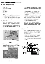
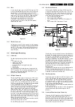
In mono sets, the signal goes via the SAW filter (position 1004
in case of QSS demodulation and 1003 in case of Intercarrier
demodulation), to the audio demodulator part of the UOC
IC7200. The audio output on pin 48 goes directly, via the smart
sound circuit (7941 for Bass and 7942 for Treble) and buffer
(7943), to the audio amplifier (AN7523 at position 7902).
The volume level is controlled at this IC (pin 9) by a
‘VolumeMute’ control line from the microprocessor.
The audio signal from IC7902 is then sent to the speaker/
headphone output panel.
Figure 9-4
9.2.3
FM radio (if present)
The FM radio uses the 10.7 MHz concept. This SIF frequency
is available at pin 10 of the tuner. Via a pre-amplifier (TS7209
and TS7210), the signal is fed for demodulation to either the
UOC (for mono FM radio) or by the Micronas MSP34X5 (for
stereo FM radio).
9.3
Video Signal Processing
9.3.1
Introduction
The video signal-processing path consists of the following
parts:
•
RF signal processing.
•
Video source selection.
•
Video demodulation.
•
Luminance/Chrominance signal processing.
•
RGB control.
•
RGB amplifier
The processing circuits listed above are all integrated in the
UOC TV processor. The surrounding components are for the
adaptation of the selected application. The I
2
C bus is for
defining and controlling the signals.
9.3.2
RF Signal Processing
The incoming RF signal goes to the tuner (pos. 1000), where
the IF signal is developed and amplified. The IF signals then
exits the tuner from pin 11 to pass through the SAW filter
(position 1002 in case of QSS demodulation and 1003 in case
of Intercarrier demodulation). The shaped signal is then applied
to the IF processor part of the UOC (pos. 7200).
Tuner AGC (Automatic Gain Control) will reduce the tuner gain
and thus the tuner output voltage when receiving strong RF
signals. Adjust the AGC take-over point via the Service
Alignment Mode (SAM). The tuner AGC starts working when
the video-IF input reaches a certain input level and will adjust
this level via the I
2
C bus. The tuner AGC signal goes to the
tuner (pin 1) via the open collector output (pin 22) of the UOC.
The IC also generates an Automatic Frequency Control (AFC)
signal that goes to the tuning system via the I
2
C bus, to provide
frequency correction when needed.
The demodulated composite video signal is available at pin 38
and then buffered by transistor 7201.
9.3.3
Video Source Selection
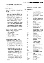
The Composite Video Blanking Signal (CVBS) from buffer
7201 goes to the audio carrier trap filters (1200, 1201, or 1202
depending on the system used) to remove the audio signal.
The signal then goes to pin 40 of IC7200. The internal input
switch selects the following input signals:
•
Pin 40: terrestrial CVBS input
•
Pin 42: external AV1 CVBS input
•
Pin 44: external Side I/O CVBS or AV2 Luminance (Y)
input
•
Pin 45: external AV2 Chrominance (C) input
Figure 9-5
Once the signal source is selected, a chroma filter calibration is
performed. The received colour burst sub-carrier frequency is
used for this. Correspondingly, the chroma band pass filter for
PAL/NTSC processing or the cloche filter for SECAM
processing is switched on. The selected luminance (Y) signal
is supplied to the horizontal and vertical synchronisation
processing circuit and to the luminance processing circuit. In
the luminance-processing block, the luminance signal goes to
the chroma trap filter. This trap is switched 'on' or 'off'
depending on the colour burst detection of the chroma
calibration circuit.
The group delay correction part can be switched between the
BG and a flat group delay characteristic. This has the
advantage that in multi-standard receivers no compromise has
to be made for the choice of the SAW filter.
9.3.4
Video Demodulation
The colour decoder circuit detects whether the signal is a PAL,
NTSC or SECAM signal. The result is made known to the auto
system manager. The PAL/NTSC decoder has an internal
clock generator, which is stabilised to the required frequency
by using the 12 MHz clock signal from the reference oscillator
of the microcontroller/teletext decoder.
The base-band delay line is used to obtain a good suppression
of cross colour effects.
The Y signal and the delay line outputs U and V are applied to
the luminance/chroma signal processing part of the TV
processor.
9.3.5
Luminance/Chrominance signal Processing
The output of the YUV separator is fed to the internal YUV
switch, which switches between the output of the YUV
separator or the external YUV (for DVD or PIP) on pins 51-53.
Pin 50 is the input for the insertion control signal called ‘FBL-1’.
When this signal level becomes higher than 0.9 V (but less than
3 V), the RGB signals at pins 51, 52 and 53 are inserted into
the picture by using the internal switches.
TUNER
RF ANT.
EXT. AUDIO
OUTPUT
EXT. AUDIO
INPUT
7902
7941
7942
7943
10
1000
11
1
1
1
AGC
18
19
23
24
68
7602
AUDIO SWITCH
VOLUME MUTE
7200
48
9
SIF
VIF
FM IF
BUFFER
FM
FMR
AVL
AUDIO
AMPL.
SMART
SND
SAW
FILTER
SAW
FILTER
SOUND
IF
DEMOD.
VISION
IF
DEMOD.
NVM
µ
P
CL 16532008_040.eps
220501
FM ANT.
0265
22
1, 12
2, 15
5, 14
FRONT AUDIO IN
AV1 AUDIO IN
AV1 AUDIO IN
7801
3, 13
7802
7901
47
30, 31
7831
CL 16532016_011.eps
120401
RGB/YUV
INSERT
RGB
56 58
VIDEO
PROC.
AUDIO
AMPL.
42
7200
V-OUT
L/R OUT
UOC
P
CRT
PANEL
MON. OUT
MAIN_OUT
24,25
SOUND
DEC
44
C-IN 45
SY_CVBS_IN
9
70
SEL-MAIN-FRNT-RR
QSS_AM_DEM_OUT
4
9
10
SC2-CTRL
40
AV1_CVBS1_1
51 53
RGB/YUV _IN
CVBS_FRONT_IN
0225-B
AV2 CVBS_IN
SVHS
Y_IN
C_IN
INTERNAL_CVBS_IN
41, 42
SC1-IN
47
Summary of Contents for L01H.1A
Page 5: ...Directions for Use EN 5 L01H 1A 3 3 Directions for Use ...
Page 7: ...Directions for Use EN 7 L01H 1A 3 ...
Page 8: ...Directions for Use EN 8 L01H 1A 3 ...
Page 9: ...Directions for Use EN 9 L01H 1A 3 ...
Page 10: ...Directions for Use EN 10 L01H 1A 3 ...
Page 11: ...Directions for Use EN 11 L01H 1A 3 ...
Page 12: ...Directions for Use EN 12 L01H 1A 3 Personal Notes ...


