background image

2 - 3

2 - 3

REPAIR INSTRUCTIONS(BD Board)

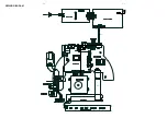
 REPAIR CHART  

A

BD Function

No Working

B

Loading

No DISC

C

All Video

No OUTPUT

A

BD function 

No working

Check CN4 cable is loose

or bad INT

Check 1.1V 1.5V 

Yes  or No output

Re-insert and fix 

the cable

YES

NO

NO

Repair BD pcb between

L1  U1 L3 U905 circuit

Check 3.3V 

Yes  or No output

YES

NO

Repair BD pcb between

U901 L2 FB19 circuit

Check Y300 Crystal 27MHz

Yes  or No output

YES

NO

Repair BD pcb between

Y300 U100 Circuit

Check U100 U201 U101  

 U102 and connect part

YES

B

Loading

No Disc

Check Y300 crystal 

27MHz Freq Yes or NO

supersession 27MHz crystal

NO

YES

OK

Check U101 U102 U201 

 and connect part

YES

Check BD Loader run

Yes or NO

supersession Loader

NO

C

Check JK805 is 

loose or bad

supersession JACK

Re-insert and fix 

the JACK

loose

Bad

Check JK805

between U100

All Video

No OUTPUT

PL

Check J800 to

BD loader Cable Loose

No

OK

Check Open/Close

Working or Not

Check J900 J901 

up!CE!Mpbefs!Dbcmf!mpptf

ps!Cbe!JOU

Check U10

And Its conjoint parts

No

ps!Cbe!JOU

Re-Insert and fix 

the cable

YES

Zft

Determine Picture Output

OK

Zft!ps!Op

Check U100 And

Their Conjoint Parts

No

Check  U10  u408

OK

Boe!Uifjs!Dpokpjou!Qbsut

D

HDMI_RX  no output

D

Ethernet No starting

Check P401 loose

or bad INT

Check P401 between U100

supersession  P401

YES

NO

INT

Repair P401 between U100

BD Board

Summary of Contents for HTB7250D

Page 1: ...d in The Netherlands Subject to modification BD Home Theater System Version1 1 TABLE OF CONTENTS Location of PCB Boards 1 2 Versions Variation 1 2 Measurement Setup 1 6 Specifications 1 3 Service Aids 1 7 ESD Safety Instruction 1 8 Lead free Soldering Information 1 9 Setting Procedure Repair Instructions 2 Disassembly Instructions Service Positions 3 Block Wiring Diagram 4 MAIN VFD SUB USB MP3 SEN...

Page 2: ...Board BD Board Touch Board Type Versions Board in used HTD7250D C C Bd 12 SERVICE SCENARIO MATRIX 12 x x x Power Board subwoofer Bd Board Level Replacement C Component Level Repair Bd HTD7255D C C Bd 12 Bd x HTB7255D 12 x x x x Bluetooth BD PCB BT PCB MAIN PCB MP3 PCB USB PCB SENSOR PCB VFD PCB TOUCH PCB Main Unit SUB PCB AMPPCB SUB _POWR CPB Subwoofer ...

Page 3: ...Kingdom Korea Latin America Australia New Zealand Russia India China A A A A C C C C Asia Pacific Taiwan File formats Audio aac mka mp3 wma wav mp4 m4a China Video avi divx mp4 m4v mkv m2ts mpg asf wmv rmvb rm rv Available only Audio formats Your home theater supports the following Extension Con tainer Audio codec Bit rate mp3 MP3 MP3 Upto 320 kbps wma ASF WMA Upto 192 kbps WMA Pro Upto 768 kbps a...

Page 4: ... H 264 AVC HiP 5 1 25 Mbps WMV9 45 Mbps m2ts in MKV container Audio codec Video codec Bit rate PCM Dolby Digital DTS core MPEG MP3 WMA AAC HE AAC DD MPEG 1 MPEG 2 40 Mbps MPEG 4 ASP 38 4 Mbps H 264 AVC HiP 5 1 25 Mbps WMV9 45 Mbps asf and wmv in ASF container Available only in Asia and China Audio codec Video codec Bit rate Dolby Digital MP3 WMA DD MPEG 4 ASP 38 4 Mbps H 264 AVC HiP 5 1 25 Mbps WM...

Page 5: ...Video Signal system PAL NTSC HDMI output 480i 576i 480p 576p 720p 1080i 1080p 1080p24 Audio S PDIF Digital audio input Optical TOSLINK Sampling frequency MP3 32 kHz 44 1 kHz 48 kHz WMA 44 1 kHz 48 kHz Constant bit rate MP3 32 kbps 320 kbps WMA 48 kbps 192 kbps Radio Tuning range Europe Russia China FM 87 5 108 MHz 50 kHz MHz 50 100 kHz Signal to noise ratio FM 50 dB Frequency response FM 180 Hz 12...

Page 6: ...Signal Disc replaces test disc 3 SBC429 4822 397 30184 Bandpass 250Hz 15kHz e g 7122 707 48001 LF Voltmeter e g PM2534 DUT RF Generator e g PM5326 S N and distortion meter e g Sound Technology ST1700B Use a bandpass filter to eliminate hum 50Hz 100Hz and disturbance from the pilottone 19kHz 38kHz Ri 50 Tuner FM MEASUREMENT SETUP ...

Page 7: ...x driver set T6 T20 4822 395 50145 Torx driver T10 extended 4822 395 50423 Compact Disc SBC426 426A Test disc 5 5A 4822 397 30096 SBC442 Audio Burn in test disc 1kHz 4822 397 30155 SBC429 Audio Signals disc 4822 397 30184 Dolby Pro logic Test Disc 4822 395 10216 SERVICE AIDS HANDLING CHIP COMPONENTS ...

Page 8: ...ore returning set to customer perform a leakage current measurement test from all exposed metal parts to earth ground to assure no shock hazard exist The leakage current must not exceed 0 5mA CLASS 1 LASER PRODUCT 3122 110 03420 GB Warning Invisible laser radiation when open Avoid direct exposure to beam S Varning Osynlig laserstrålning när apparaten är öppnad och spärren är urkopplad Betrakta ej ...

Page 9: ...duce heat Mix of lead free solder alloy parts with leaded solder alloy parts is possible but PHILIPS recommends strongly to avoid mixed solder alloy types leaded and lead free If one cannot avoid or does not know whether product is lead free clean carefully the solder joint from old solder alloy and re solder with new solder alloy SAC305 Use only original spare parts listed in the Service Manuals ...

Page 10: ...our home network condition 5 Follow the onscreen instructions to confirm the update Update process takes about 5 minutes to complete Once complete the home theater automatically switches off and restarts If it does not disconnect the powercord for a few seconds and then reconnect it w w w LAN N I I M D H C R A I M D H Bottom side view of OPU CAUTION This information is confidential and may not be ...

Page 11: ...CN601 CN1 And Their Conjoint Parts No Check IC1 OK And Their Conjoint Parts B C D F G I J Re insert and fix the cable Check IC304 Pin5 14 36 approx 5V Pin46 approx Check R312 R313 R377 Re insert and fix OK Check CN201 Yes Yes 3 3V Yes or No Loose or bad INT Check R314 R358 R375 OK Check IC305 Pin3 19 22 No approx 3 3V And Its Conjoint Parts Re insert and fix the cable Check BD Board See Contents B...

Page 12: ... or NO supersession 27MHz crystal NO YES OK Check U101 U102 U201 and connect part YES Check BD Loader run Yes or NO supersession Loader NO C Check JK805 is loose or bad supersession JACK Re insert and fix the JACK loose Bad Check JK805 between U100 All Video No OUTPUT PL Check J800 to BD loader Cable Loose No OK Check Open Close Working or Not Check J900 J901 up CE Mpbefs Dbcmf mpptf ps Cbe JOU Ch...

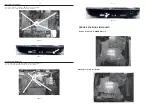
Page 13: ...n 5 screws E at the DVD Module as shown in figure 5 Figure 4 Figure 5 Figure 6 Dismantling of the MP3 USB SENSOR Board 1 Loosen 3 screws F on the top of MP3 USB Board as shown in figure 6 2 Loosen 2 screws G on the top of SENSOR Board as shown in figure 7 Figure 7 Note In some service positions the components or copper patterns of one board may risk touching its neighbouring pc boards or metallic ...

Page 14: ... back panel as shown in figure 9 SERVICE POSITIONS MAIN UNIT Figure 10 Figure 8 Figure 9 Service Position A MAIN BD Board Service Position E All Boards Dismantling of the MAIN Board 1 Loosen 6 screws J on the top of main board as shown in figure 10 2 Loosen 2 screws K at the back panel as shown in figure 11 Figure 11 H I J K ...

Page 15: ...igure 19 S Figure 19 SERVICE POSITIONS SUBWOOFER DISASSEMBLY INSTRUCTIONS SUBWOOFER Dismantling of the Subwoofer Rear Panel 1 Loosen 9 screws Q at the subwoofer rear panel as shown in figure 17 Dismantling of the Power Board 1 Loosen 5 screws R on the top of power board as shown in figure 18 R Figure 17 Figure 18 Q ...

Page 16: ...n 5 screws E at the DVD Module as shown in figure 5 Figure 4 Figure 5 Figure 6 Dismantling of the MP3 USB SENSOR Board 1 Loosen 3 screws F on the top of MP3 USB Board as shown in figure 6 2 Loosen 2 screws G on the top of SENSOR Board as shown in figure 7 Figure 7 Note In some service positions the components or copper patterns of one board may risk touching its neighbouring pc boards or metallic ...

Page 17: ... back panel as shown in figure 9 SERVICE POSITIONS MAIN UNIT Figure 10 Figure 8 Figure 9 Service Position A MAIN BD Board Service Position E All Boards Dismantling of the MAIN Board 1 Loosen 6 screws J on the top of main board as shown in figure 10 2 Loosen 2 screws K at the back panel as shown in figure 11 Figure 11 H I J K ...

Page 18: ...igure 19 S Figure 19 SERVICE POSITIONS SUBWOOFER DISASSEMBLY INSTRUCTIONS SUBWOOFER Dismantling of the Subwoofer Rear Panel 1 Loosen 9 screws Q at the subwoofer rear panel as shown in figure 17 Dismantling of the Power Board 1 Loosen 5 screws R on the top of power board as shown in figure 18 R Figure 17 Figure 18 Q ...

Page 19: ...ner Pack Tuner Audio TPIC2050 Motor driver SERVO UART UART2 0R Jump 0R Jump Simple Advance MP3 Mic Delect MP3 Mic Detect Mic Mono Jack 7 0A MOSFET SW IC CEM8311 AO4813 Motor driver 12V 5V Motor driver USB WiFI H L Power SW control TAS5538 D AMP PWM FL VOLUME FL TAS5612A PWR AMP OUTPUT 30 270W FR FL RR RL SPK ohm SUB 135W 5 FR FL RR RL C SUB SRR SRL I2C MCLK H I2S 1 8V 3 3V LDO Reg LM1117 33 33V 12...

Page 20: ...4 2 4 2 WIRING DIAGRAM V1 V4 V2 V3 V5 SV2 V10 CN901 AC SOCKET SV1 ...

Page 21: ...C Multibit Oversampling ADC Low Latency Anti Alias Filter High Pass Filter High Pass Filter Stereo Input 1 Serial Audio Output 3 3 V 5 V MUX e c a f r e t n I l a i r e S M C P Register Configuration l e v e L r o t a l s n a r T Stereo Input 2 Stereo Input 3 Stereo Input 4 Mic Input 1 2 Stereo Input 5 Stereo Input 6 PGA 32 dB 32 dB r o t a l s n a r T l e v e L Reset I C SPI Control Data Interrup...

Page 22: ...e D h p m E C R S M W P S N 0 t e D 7 s d a u q i B C R D Loud p m o C t f o S e n o T C D k c o l B e D h p m E C R S M W P S N 0 t e D 7 s d a u q i B C R D Loud p m o C t f o S e n o T C D k c o l B e D h p m E C R S M W P S N 0 t e D 7 s d a u q i B C R D Loud p m o C t f o S e n o T C D k c o l B e D h p m E C R S M W P S N 0 t e D 7 s d a u q i B C R D Loud p m o C t f o S e n o T C D k c o ...

Page 23: ...B TDQ NPTJ UP 5 6424 235Qjo UP 5 6424 234Qjo ETQ JSR Q NVUF CL4 4W CL4 4W efcvh2 efcvh3 efcvh4 efcvh5 efcvh6 CL4 4W CL4 4W CL4 4W CL4 4W CL4 4W C215 100P C214 100P R282 4 7K R278 33 CL4 4W T1 2 T2 3 T3 4 HOE 5 TEB 6 TDM 7 XD 8 WDD 9 IC202 RCI024004 0005 C213 104 CL4 4W efcvh3 efcvh4 efcvh5 efcvh6 R223 10K R273 10K UP 5 6424 5Qjo UP DO 2Qjo UP DO 3Qjo UP UP UP R274 10K R262 33 R263 33 R261 33 R247 ...

Page 24: ... C4158 C218 R3002 R3001 C3001 C3002 C3003 C3004 C4144 C4142 D4171 C4130 FB5102 FB5101 R4111 C727 C4110 R4105 R4103 R4106 R721 C730 C729 C4113 C4107 C4108 C4112 R4128 R4104 R4120 R4119 R4116 R4115 R4114 R4113 C4129 R5113 C5114 C5341 R5041 C4111 C4172 C4171 Q4172 R4174 Q4171 R4171 R4173 C4120 C4119 C4118 C4117 C4124 C4123 R4112 C4154 C5132 R5118 R4122 R5044 R4183 Q4181 C1029 FB202 C4004 C352 R344 R2...

Page 25: ...5317 C5318 C5325 C5326 C5327 C5328 C5329 C5330 R5312 R5314 R5315 C221 C502 R505 R504 Q502 Q501 D501 R401 C405 C5342 C2001 C2002 C2003 C2004 C2005 C2006 C2007 C2008 C2009 C2010 C2011 C327 C330 C331 C351 R3028 R4143 C320 C4155 C4131 R4142 R4144 C722 R4107 D502 C203 C209 R2023 C208 D201 D202 Q201 R210 R209 R2021 R2022 D306 D307 C5343 C705 FB832 FB831 C854 C853 C852 C851 ZD701 R702 C707 C706 C704 C703...

Page 26: ...pcs DDR3 64MB x 16 x 2 pcs DDR3 CEC CEC HDMI OUT IENJ BSD Gspn UW NAND Flash 2G bit 256MB HDMI TMDS connect to main board HA500 VBSU SY0UY J3D J3D JSR Atheros RT3370 Wifi Module BRAND ALPHA Model Number WUS N18M J3D NDML CDL MSDL SY EBU JO CEC SY NDML SY CDL SY MSDL EBU10203 PVU USB2 0 Bus front USB2 0 USB2 0 Bus back USB2 0 DC TO DC DC TO DC 5V 1 2V 2 6A 3 3V 1 1A TPS54418 1 5V 1 65A STBY_3 3V 0 ...

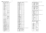
Page 27: ...10 MCLK 11 GND 12 SDA 13 SCL 14 AMUTE high and low cotrol 15 CEC 16 I2C_IRQ high and low cotrol 17 GND 18 IR I 19 IPOD_RXD 20 IPOD_TXD 21 ADC_RST working High reset low 22 SPDIF_RST working High reset low 23 SPDIF_IRQ high and low cotrol 24 RX_DATA0 25 GND 26 RX_BCK 27 RX_LRCK 8 2 RX_MCLK 29 GND 30 SPDIF_ARC 31 GND 32 3 HDMI_RX_SDA NC 33 HDMI_RX_SCL NC 34 HDMI_RX_HPD NC 35 RX5V_IN2 NC 36 RXHPD CTL...

Page 28: ...6 3 6 3 Waveforms for measure point ...

Page 29: ...6 4 6 4 Waveforms for measure point ...

Page 30: ...7 1 7 1 TOUCH BOARD TABLE OF CONTENTS Circuit Diagram 7 2 PCB Layout Top Bottom View 7 3 ...

Page 31: ...ead 1 IC1 IC_EKT4701_P32 R25 0 R29 0 R28 0 PGM_DAT PGM_CLK DRV0 DRV1 DRV2 DRV3 PGM_CLK 5 5V_LED BK3V3 DAT CLK SEN1N SEN0N SEN0 N SEN1 N 3VDD L_POWE R L_POWE R L_VOL L_SOURCE L_SOURCE L_PLAY L_PLAY L_OPEN L_OPEN L_STOP L_VOL L_STOP Pxy_VF Pxy_TP B Pxy_VF Pxy_TP A Pxy_TP B I2C_DAT I2C_DAT I2C_CLK 1 2 1 2 1 2 1 2 1 2 1 2 1 2 1 2 1 2 3 4 5 DRV DRV DRV DRV DRV DRV DRV 1 2 3 4 5 6 7 8 1 2 1 1 SEN1 P 24 ...

Page 32: ...DAT LCK GND PGM_CLK RESET PGM_DAT GND HTS9221_self_ISP_V02_0928 5 5V RB1 R27 R26 R25 Q1 C15 C1 C2 C4 C5 C6 C7 C8 C9 C10 C11 C12 C13 C14 D1 D2 D3 D4 D5 D6 D7 D 8 D9 D10 R1 R2 R3 R4 R5 R6 R7 R 8 R9 R10 R11 R13 R14 R15 R16 R17 R18 R19 R20 R21 R22 R23 CN1 IC1 R12 R24 R28 R29 k a a k k a a k k a a k k a a k a k ...

Page 33: ...8 1 8 1 POWER BOARD TABLE OF CONTENTS Internal IC Diagram 8 1 Circuit Diagram 8 2 PCB Layout Top View 8 3 PCB Layout Bottom View 8 4 IC903 INTERNAL IC DIAGRAM SSC620S IC905 INTERNAL IC DIAGRAM AZ7500BP ...

Page 34: ... S G Q901 7N60C C918 M103P OCP 6 GND 8 PB OLP 1 Drive 5 Vcc 2 FM 7 STARTUP 4 NC 3 IC903 SSC620S D925 1N4148S E C B Q908 2SC945 C930 CC104P 1 2 3 4 5 6 7 8 9 CN904 CN9P 25 14V PWM Reset SGND SGND VCC2 HVCC 6 4 8 5 10 11 9 2 1 12 T901 ER 28 6 6 BKVcc SGND ON OFF AMP_VCC SGND AMP_VCC SGND 1 2 3 4 5 6 7 8 9 10 11 12 13 14 CN903 14V PWM Reset AGND SGND 14V R947 680 R948 680 R949 680 R946B 680 R946A 680...

Page 35: ...3 J914 J915 J916 J917 J918 J920 J921 J922 DIP SECONDARY PRIMARY D1 D2 C991 P908 R908A D907 D908 C912 C908 R929 R930 R924 CN904 C918 C916 D913 R911 D903 L903 Q902 R917 T901 CN901 D901 R915 R926 R918 TVR903 L902 L901 L907 GT904 D917 C989 C999 C990 C988 C975 C974 C969 C968 C966 D906 TVR902 TVR901 BD901 C910 C925 C932 C923 D905 GT901 GT902 GT903 IC905 NTC901 P906 R912 R916 R920 CN902 C952 Q903 C987 P9...

Page 36: ...R932 R931 R908 D912 C931 C 9 4 7 C946 C945 C930 C 9 3 7 C 9 2 1 ZD908 C924 C951 C956 C957 C961 C962 C963 C964 C967 D909 D910 D 9 1 6 D918 Q906 Q912 R955 R956 R958 R961 R962 R964 R965 R968 R969 R970 R971 R972 R973 R974 R978 ZD910 Z D 9 1 3 R940 R951 R 9 5 4 C948 C903 ZD909 C926 R952 ZD907 C902 C901 R904 Z D 9 0 5 ZD904 ZD903 R937 R936 R925 R909 C944 C 9 1 4 R921 R914 R913 R910 R907 R905 R902 R901 D...

Page 37: ...hanical Exploded View Main Unit 1 2 2 3 4 5 6 7 8 9 21 21 22 22 23 23 24 24 25 25 26 26 27 27 28 28 29 29 2 2 31 31 32 32 33 33 34 34 35 35 T2 T3 T4 T5 T6 T8 T9 T21 T23 T T7 T22 Note A1 12 4 7 8 9 25 SW2 25 FM RC V6 ...

Page 38: ...10 2 10 2 Mechanical Exploded View Subwoofer SW1 SW2 SW3 SW4 SW12 SW13 SW5 SW6 SW7 SW8 SW9 SW10 SW11 ...

Page 39: ...10 1 REVISION LIST Version 1 0 Initial release Version 1 1 Add HTB7255D 12 version ...

Reviews: