background image

PG-1810 Service Manual  


PANTECH                                              R&D CONFIDENTIAL 

21


4.2.4.2  Transmitter Part 

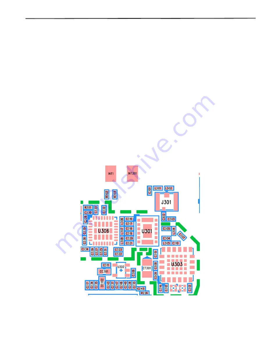
A. 6dB attenuators : U304, U305 

        These passive components are adopted for PAM to operate in a stable output power. 

B.  Antenna Switch Module With SAW Filter : U301 

These filters pass through the signals of which frequency band of 824~849MHz, 

1710MHz~1785MHz, 1850MHz~1910MHz which is the transmit frequency of GSM850, DCS, 

PCS system terminal, and it suppresses other images and spurious frequencies when the 

terminal transmits GMSK modulated frequencies. 

C. Power AMP Module(PAM) : U303 

This device amplifies signals ahead of transmiting them through the antenna to provide a 

sufficient RF power. It has amplification factor of 28dB and efficiency of about 53% typically in GSM 

band and amplification of 27dB and efficiency of about 53% typically DCS/PCS band. 

D. RF Switch connector : J301 

RF Switch connector used to test Mainboard’s RF characteristics and to calibrate. 


E. Antenna: Antenna Contact Plate : INT301 

This device enables signals to be transmitted and received from BTS by Um interface. 

External Antenna can be contacted with Mainboard through Antenna Contact Plate. 


Fig.4-9. Transmit part PCB Layout 

Summary of Contents for PG-1810

Page 1: ...1810 Service Manual GSM Cellular Phone Pantech Co Ltd Korea February 22 2006 1st Edition For Use by Authorized Service Maintenance Personal Only Documents to Receive This Addendum PG 1810 Maintenance...

Page 2: ...6 4 2 3 RECEIVE SECTION 17 4 2 3 1 AN OVERVIEW OF RECEIVE SECTION 17 4 2 3 2 RECEIVER PART 19 4 2 4 TRANSMIT SECTION 20 4 2 4 1 AN OVERVIEW OF TRANSMIT SECTION 20 4 2 4 2 TRANSMITTER PART 21 4 2 5 OFF...

Page 3: ...4 Charger part 41 6 4 1 Charging error 41 6 5 CAMERA SENCE PART 43 6 5 1 CAMERA PREVIEW ERROR ALL ITEMS ARE ON LCD MODULE 43 6 6 Blutooth 45 6 7 RF PART 47 6 7 1 TEST CONDITIONS 47 6 7 2 POWER SUPPLY...

Page 4: ...y management The MS and the BS subsystem communicate across the Um interface also known as radio link The specifications relating to MS are as follows TS 100 607 1 Digital cellular telecommunication s...

Page 5: ...ata rate feature are used appropriately to ensure its best performance This product consists of a handset battery pack and Travel charger 1 4 Characteristics 1 All the active devices of PG 1810 are ma...

Page 6: ...ut Power 33 2 30 2dBm 30 2dBm Frequency Error 90Hz 180Hz 190Hz Phase Error RMS 5 PEAK 20 Minimum Output Power 5 5 0 5dBm Power Control 5 19 0 15 2 dB Step Output RF Spectrum TS 100 910V6 2 0 Switching...

Page 7: ...NTECH R D CONFIDENTIAL 6 Section 3 Operation 3 1 Name of each part Main Display Screen Speaker Intenna Sub Display Screen 330K Pixel Camera Battery MIC Receiver KEY PAD Ear Jack Micro SD CARD Side Key...

Page 8: ...acters Driver CL761AP Core Logic Module Dimen 34 4 H x 54 13 V x 3 5 D Active Area 1 04 inches Resolution pixels 96 x 96 pixels Color Display Depth 16 bits 3 3 Keypad Market Goal Projected Actual Comm...

Page 9: ...PG 1810 Service Manual PANTECH R D CONFIDENTIAL 8 3 4 BLUETOOTH MODULE...

Page 10: ...voltage and pressing END key on the key pad short circuits Ground and _ PowerON AD6535 U202 control that power manage regarding power on off in handset Pressing POWERKEY on the key pad is active on t...

Page 11: ...h ROM SRAM AD6535 VBC Chip AD6528D is GSM ASIC chipset implemented for GSM terminal s system control and baseband digital signal processing Major parts used in the logic part are as follows 1 AD6528D...

Page 12: ...ng of terminal chips The function and characteristics of clock are as follows 1 Complete single chip GSM Processor 2 Channel codec sub system Channel coder and decoder Interleaver and Deinterleaver En...

Page 13: ...sing part in GSM mode consisting of speech transcoding and Channel equalization as follows 1 Speech transcoding In full rate the DSP receives the speech data stream from VBC and encodes data from 104k...

Page 14: ...GSM handset requires serial connections to provide data during normal phone operation Manufacturing testing and debugging 7 General Purpose Interface The AD6528D provides 32 interface pin for control...

Page 15: ...unding alert melody tones The melody datas are stored in flash memory U203 And generated by Melody IC U117 2 Vibrator This is a device enabling vibration The vibrator data is stored in flash memory U2...

Page 16: ...solution cost and reduced complexity The baseband interface is compatible with any supplier s baseband subsystem The transmit section is a complete up conversion path from the baseband subsystem to t...

Page 17: ...The battery voltage in return is applied to the logic part and RF part via LDO Low Drop Out regulator As several LDO regulators are used power can be supplied for each necessary part efficiently Audi...

Page 18: ...PG 1810 Service Manual PANTECH R D CONFIDENTIAL 17 Table 4 1 Pin Description of Si4210 GM 4 2 3 Receiver Section 4 2 3 1 An Overview of Receive section Fig 4 6 Receiver block diagram...

Page 19: ...utomatically selected by the ARFCN 9 0 bits and the BANDIND bit in Register 21h If performing LNA swapping the LNASWAP bit in Register 05h is also needed The LNA gain is controlled with the LNAG bit i...

Page 20: ...equency band As an example the RFIA inputs and GSM 850 LNA are used for E GSM 900 operation 4 2 3 2 Receiver Part Antenna Swithch Module with SAW Filter U301 FEM Front End Module consists of Tx filter...

Page 21: ...ure BQP BQN baseband signals to an intermediate frequency IF that is filtered and which is used as the reference input to the OPLL The OPLL consists of a feedback mixer a phase detector a loop filter...

Page 22: ...transmits GMSK modulated frequencies C Power AMP Module PAM U303 This device amplifies signals ahead of transmiting them through the antenna to provide a sufficient RF power It has amplification fact...

Page 23: ...Programming the N Divider register for either RF1 or RF2 automatically selects the proper VCO The output frequency of each PLL is as follows fOUT N f The DIV2 bit in register 31h controls a programma...

Page 24: ...PG 1810 Service Manual PANTECH R D CONFIDENTIAL 23 Fig 4 11 Top view of VCTCXO part on the PCB artwork...

Page 25: ...ion Test Set Agilent Technologies 8593E Spectrum Analyzer Hewlett Packard TDS 3054B Oscilloscope Tektronix FLUKE 87 Digital Multimeter Fluke E3630A DC Power Supply Hewlett Packard Others Accessory Int...

Page 26: ...PANTECH R D CONFIDENTIAL 25 SECTION 6 Equipment Repair Procedure 6 1 1 Power CHECK 1 Check battery power 3 5V 4 2V 2 Check to see if U202 CC201 pin voltage is same with battery power CP100 BATTERY PA...

Page 27: ...PG 1810 Service Manual PANTECH R D CONFIDENTIAL 26 3 Check to see if U202 A4_B4 T2_T3 P1_N1 D16 and T7 pin is 2 8V 2 8V 1 8V 2 75V and 1 8V CP101 CP101...

Page 28: ...PG 1810 Service Manual PANTECH R D CONFIDENTIAL 27 4 Check to see if U202 T14 and R121 pin becomes to 0V CP102 Pressing END key to turn on equipment CP102...

Page 29: ...Oscillation CHECK 1 Check to see if U201 A3 and B3 pin is oscillated 32 768KHz CP103 NO Check R205 and then replace X1 2 Check to see if U201 N10 and C201 pin Master Clock 26MHz CP104 NO Check C1 2 p...

Page 30: ...is around 2 8V CP105 NO Check U201 2 Check to see if U121 3 pin or CC119 are around 3 3V CP106 NO Check to see if U121 1 pin is around 3 5V 4 2V NO Replace U121 3 Check to see if D101 119 or around r...

Page 31: ...cklight Not in Operation White 1 Check to see if RV1 s Voltage On LCD Module is 2 8V and C16 s Voltage On LCD Module is 3 5V 4 2V CP108 Check to see if RV1 s Voltage On LCD Module is 4V CP109 NO Repla...

Page 32: ...Hands free Earphone Microphone Hands free Mic 6 2 1 No receiving tone heard Ear piece 1 Check C243 U202 J15 R219 and K15 R220 pins C237 Ear Signal for waveform CP110 NO Replace U202 and C243 C237 2 Ch...

Page 33: ...U117 E2 pin s input Clock 26MHz CP113 NO Check to see U116 and U307 cold solder broken short to the other PCB pattern or not If you find out any defect you replace it 4 Check to see U117 B6 A65 pin s...

Page 34: ...PG 1810 Service Manual PANTECH R D CONFIDENTIAL 33 CP111 CP115 CP116 CP113 CP112 CP114 CP115 CP115 CP116...

Page 35: ...18 NO Check that U201 or U117 is cold solder broken short to the other PCB pattern or not 3 Check U102 5 9 pin for waveform CP119 NO Check that U102 is cold solder broken short to the other PCB patter...

Page 36: ...k that U201 R227 Q203 R234 R235 are cold solder broken short to the other PCB pattern or not If you find out any defect you replace it 2 Check to see if Q203 E and C pin are 0V during pressing Hook Sw...

Page 37: ...nd 1 5V CP125 NO Check that S216 C257 C250 and R228 are cold solder broken short to the other PCB pattern or not If you find out any defective part you replace it Set to HP8960 to connect a call and t...

Page 38: ...not connected that Voltage is around 0V NO Check to see U202 N16 or R223 C252 cold solder broken short to the other PCB pattern or not If you find out any defective part you replace it Set to HP8960 t...

Page 39: ...2 pin is 2 8V CP129 NO Check to see U201 2 Check to see if U111 3 pin is 3 5 4 2V CP130 NO Check to see U111 cold solder broken short to the other PCB pattern or not If you find out any defect you rep...

Page 40: ...CP131 NO Check to see U202 T6 pin and C239 cold solder broken short to the other PCB pattern or not If you find out any defect you replace it 2 Check to see U109 12 13 and 15 pin for wave form CP132 N...

Page 41: ...t any defect you replace it 2 Check to see if J103 1 pin is around GND CP134 NO Check to see U109 and R143 cold solder broken short to the other PCB pattern or not If you find out any defect you repla...

Page 42: ...the other PCB pattern or not If you find out any defect you replace it 2 Check to see Q201 3 4 7 and 8 are low 0V CP137 NO Check to see U202 and R121 cold solder broken short to the other PCB pattern...

Page 43: ...PG 1810 Service Manual PANTECH R D CONFIDENTIAL 42 CP137 CP138 CP136...

Page 44: ...roken short to the other PCB pattern or not If you find out any defect you replace it 3 Check to see if U3 3 pin and L2 are around 2 8V CP140 NO Check to see U3 L2 and C24 cold solder broken short to...

Page 45: ...PG 1810 Service Manual PANTECH R D CONFIDENTIAL 44 CP140 CP139 CP141...

Page 46: ...fect you replace it 3 Check To see Audio Gateway is enabled Check to see if U113 8 9 and U115 8 9 pin are low and U113 2 pin PCM CLK U110 4 pin PCM SYNC CP144 NO Check to see cold solder broken short...

Page 47: ...PG 1810 Service Manual PANTECH R D CONFIDENTIAL 46 CP145...

Page 48: ...ode Ch190 Power Level 13 3 Test condition 3 Traffic channel DCS Band Tx mode Ch698 Power Level 10 4 Test condition 4 Traffic channel GSM850 Band Rx mode Ch190 Input power 70dBm 5 Test condition 5 Traf...

Page 49: ...r not If you find out any defect you replace it 3 Check to see U307 3 pin s output Clock 26MHz CP148 NO Check to see U307 cold solder broken short to the other PCB pattern or not If you find out any d...

Page 50: ...PG 1810 Service Manual PANTECH R D CONFIDENTIAL 49 CP147 CP148 CP149...

Page 51: ...PG 1810 Service Manual PANTECH R D CONFIDENTIAL 50 CP150...

Page 52: ...r not If you find out any defect you replace it 2 Check to see C324 C326 C238 and U302 1 2 3 pin s signal CP 152 NO Check to see U201 U302 cold solder broken short to the other PCB pattern or not If y...

Page 53: ...short to the other PCB pattern or not If you find out any defect you replace it 2 Check to see C308 U303 18 pin s Voltage 2 8 V and C309 U303 20 pin Voltage 0 1 3V CP 155 NO Check to see U201 U303 C3...

Page 54: ...SM U301 1 2pin DCS U301 3 4 pin PCS U301 5 6pin is same CP 157 NO Check to see U301 cold solder broken short to the other PCB pattern or not If you find out any defect you replace it 6 7 5 2 TX Parat...

Reviews: