background image

10.1.2.  Sub-Contrast adjustment

Name  of measuring  instrument

Connection

Remarks

RF  generator

Base Band signal generator 
HD signal generator

Steps

Remarks

Adjustment of TV (RF  system)

Note:

In adjustment,  you  must setting to  modulation of signal  at 90%.

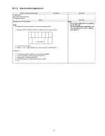
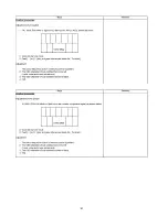
1.  Receive  a  RF  PAL  100%  Full White or Split  Colour bar shown  as below.

Note:

Sub-contrast adjustment is unadjusted


for AV/ HD  input.

But, when  needing the adjustment cho­

sen  manually, please refer to [ alterna­

tive method  ].

100% White

2.  Goes into  service  mode.
3.  Push  a  [  1  ] or [ 2 ]  key, and  goes into service  mode for [ CONTRAST ]. 

Adjustment

1.  The colour key yellow button of remote control  is pushed.

2.  The  OSD  character of sub-contrast becomes red.

(Inside  under automatic adjustment)

3.  The  OSD  character of sub-contrast  returns to  black.
4.  End.

35

Summary of Contents for TX-PR65VT20

Page 1: ... attempt to service or repair the product or products dealt with in this service information by anyone else could result in serious injury or death IMPORTANT SAFETY NOTICE There are special components used in this equipment which are important for safety These parts are marked by A in the Schematic Diagrams Circuit Board Diagrams Exploded Views and Replacement Parts List It is essential that these...

Page 2: ...MAIN Board 3 3 Schematic Diagram 52 13 5 P SUB Board Schematic Diagram 53 13 6 A Board 1 25 Schematic Diagram 54 13 7 A Board 2 25 Schematic Diagram 55 13 8 A Board 3 25 Schematic Diagram 56 13 9 A Board 4 25 Schematic Diagram 57 13 10 A Board 5 25 Schematic Diagram 58 13 11 A Board 6 25 Schematic Diagram 59 13 12 A Board 7 25 Schematic Diagram 60 13 13 A Board 8 25 Schematic Diagram 61 13 14 A Bo...

Page 3: ...nd such as a w ater pipe as shown in Figure 1 3 Use Leakage Current Tester Simpson 228 or equivalent to measure the potential across the measuring network 4 Check each exposed metallic part and measure the voltage at each point 5 Reserve the AC plug in the AC outlet and repeat each of the above measure 6 The potential at any point TOUCH CURRENT expressed as voltage U1 and U2 does not exceed the fo...

Page 4: ...re of the assembly 3 Use only a grounded tip soldering iron to solder or unsolder ES devices 4 Use only an anti static solder removal device Some solder removal devices not classified as anti static ESD protected can generate electrical charge sufficient to damage ES devices 5 Do not use freon propelled chemicals These can generate electrical charges sufficient to damage ES devices 6 Do not remove...

Page 5: ... the melting point is 50 70 F 30 40 C higher Please use a high tem perature soldering iron and set it to 700 20 F 370 10 C Pb free solder will tend to splash when heated too high about 1100 F or 600 C If you must use Pb solder please com pletely remove all of the Pb free solder on the pins or solder area before applying Pb sol der If this is not practical be sure to heat the Pb free solder until i...

Page 6: ...mitter D Format Converter Plasma AI Sub Field Processor Board Name Function C1 Data Driver Lower Right C2 Data Driver Lower Center C3 Data Driver Lower Left C4 Data Driver Upper Right C5 Data Driver Upper Center C6 Data Driver Upper Left SC Scan Drive SS Sustain Drive SS2 Sustain out Upper SS3 Sustain out Lower SU Scan out Upper Non serviceable SU Board should be exchanged for service SD Scan out ...

Page 7: ...z 31 44 59 89 1 024 x 768 60 Hz 48 36 60 00 1 024 x 768 70 Hz 56 48 70 07 1 024 x 768 75 Hz 60 02 75 03 1 024 x 768 85 Hz 68 68 85 00 1 280 x 768 60 Hz 47 70 60 00 1 280 x 1 024 60 Hz 63 98 60 02 1 366 x 768 60 Hz 48 39 60 04 Macintosh13 640 x 480 35 00 66 67 Macintosh16 832 x 624 49 73 74 55 Macintosh21 1 152 x 870 68 68 75 06 PC from HDMI term inal Applicable input signal for PC is basically com...

Page 8: ... M NTSC Video recorders VCR Playback from NTSC Video recorders VCR Digital terrestrial services MPEG2 and MPEG4 AVC H 264 Check the latest information on the available services at the following website English only http panasonic jp support global cs tv VHF UHF Temperature Humidity 0 C 35 C 20 80 RH non condensing 21 Pin terminal Audio Video in Audio Video out RGB in Q Link 21 Pin terminal Audio V...

Page 9: ...onic Main body Resin Lens Liquid crystal glass within approx 3 2 m from the front of the TV 0 C 40 C 177 mm x 46 mm x 174 mm 63 0 g Net Viewing range Operating Conditions Dimensions W x H x D Mass including battery Note Design and Specifications are subject to change without notice Mass and Dimensions shown are approximate 9 ...

Page 10: ...om the PC starts with a STX signal followed by the com m and the param eters and lastly an EXT signal in that order If there are no parameters then the parameter signal does not need to be sent Please see other side regarding Com m ands and Parameters Connection STYX Command 3 byte fixed Colon and Parameter are only sent when necessary End 03 h 1 byte C1 I C2 I C3 Ш P1 P2 I РЗ I P4 I P5 I I EX I S...

Page 11: ...H UP CHU SELECT CH DOWN CHD TV IMS TV QMI QMI TV TV network Toggle Analogue TV IMS TVA TVA DVB T IMS TVD TVD DVB S Other Sat IMS BS1 BS1 Freesat IMS BS2 BS2 DVB C IMS CAB CAB Component 1 IMS C1 C1 Component2 IMS C2 C2 Video 1 IMS V1 V1 Video 2 IMS V2 V2 Video 3 IMS V3 V3 S Video 1 IMS S1 S1 SCART Cable S Video 2 IMS S2 S2 SCART Cable HDMI 1 IMS H1 H1 HDMI 2 IMS H2 H2 HDMI 3 IMS H3 H3 HDMI 4 IMS H4...

Page 12: ...F 480i 480p 576i 576p 720p 1080i 1080p DIRECT CH INPUT 0 ICH 0 1 ICH 1 2 ICH 2 3 ICH 3 4 ICH 4 5 ICH 5 6 ICH 6 7 ICH 7 8 ICH 8 9 ICH 9 MENU FUNCTION MENU MEN SELECT SEL RETURN RTN EXIT EXT ARROW LEFT ARL ARROW RIGHT ARR ARROW UP ARU ARROW DOWN ARD OPTION SUB MENU SUB RED RED GREEN GRN YELLOW YEL BLUE BLU VIERA TOOLS VTL 12 ...

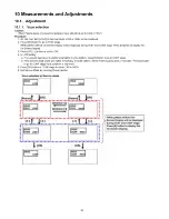
Page 13: ...DATA OPTION 4 STBY SOFT Model ID STBYEEP STBY ROMCOR PDPSOFT R E Cnt PDPEEP PDP DCC CMS data PDP PDPOM FRC EEP MIFO SOFT Ajax_CE I Sub Item I Ia d j u s t i CONTRAST OOOOi YMAX 6 1 1 Key command 1 button Main items Selection in forward direction 2 button Main item s Selection in reverse direction 3 button Sub items Selection in forward direction 4 button Sub item s Selection in reverse direction R...

Page 14: ...10 OPT 3 00000001 OPT 4 01000000 EDID CLK MID MIRROR 00 See next VSUS LOW AGING ALL WHITE Built in test patterns can ALL BLUE WITH WHITE OUTSIDE FRAME be displayed ALL GREEN ALL RED LOW STEP WHITE LOW STEP BLUE LOW STEP GREEN LOW STEP RED WHITE DIAGONAL STRIPE RED DIAGONAL STRIPE GREEN DIAGONAL STRIPE BLUE DIAGONAL STRIPE A ZONE B ZONE 1 WINDOW COLOR BAR 9 POINTS BRIGHT MEASURE 2 DOT OUTSIDE FRAME...

Page 15: ... 00 00 Time 00000 40 On Off 0000022 POWER ON TIME COUNT Press MUTE button 3 sec 6 3 2 Display of SOS History SOS History Num ber of LED blinking indication From left side Last SOS before Last three occurrence before 2nd occurrence after shipment 1st occurrence after shipment This indication will be cleared by Self check indication and forced to factory shipm ent setting 6 3 3 POWER ON Time On Off ...

Page 16: ... a last memory However Euro model is compulsorily set to TV AVnS AVnC only Euro model selectable PC selectable with VGA option Initial POS Select programme number Selection Off 0 to 99 Off give priority to a last memory Initial VOL level Adjust the volume when each time power is switched on Selection Range Off 0 to 100 Off give priority to a last memory Maximum VOL level Adjust maximum volume Rang...

Page 17: ...be copied User setting data incl Hotel mode setting data Channel scan data 6 5 2 Preparation Make pwd file as startup file for a or b in a empty SD card 1 Insert a empty SD card to your PC 2 Right click a blank area in a SD card window point to New and then click text document A new file is created by default New Text Document txt 3 Right click the new text docum ent that you just created and sele...

Page 18: ...wing password for a or b by using remote control a For Board replacem ent 2770 b For Hotel 4850 Data will be copied from TV set to SD card It takes around 2 to 6 minutes maximum for copying 4 After the completion of copying to SD card remove SD card from TV set 5 Turn off the TV set Note Following new folder will be created in SD card for data from TV set a For Board replacement user_setup b For H...

Page 19: ...rom SD card to TV set 4 After the completion of copying to SD card remove SD card from TV set a For Board replacem ent Data will be deleted after copying Limited one copy b For Hotel Data will not be deleted and can be used for other TVs 5 Turn off the TV set Note 1 Depending on the failure of boards function of Data copy for board replacem ent does not work 2 This function can be effective among ...

Page 20: ...and while pressing VOLUME button on the main unit press MENU button on the remote con trol for more than 3 seconds 7 1 2 Screen display 7 1 3 Check Point Confirm the following parts if NG was displayed Display Ref No Description P C B TUN TU2901A TUNER A Board STBY IC1100 MPU A Board MEM1 IC1101 EEPROM MPU A Board MEM2 IC8950 EEPROM PEAKS LDA2 A Board ADAM IC8000 А chip PEAKS LDA2 A Board AVSW IC3...

Page 21: ...Flashing timing chart 2 Contents W hen an abnorm ality has occurred the unit the protection circuit operates and reset to the stand by mode At this time the defective block can be identified by the num ber of blinks of the Power LED on the front panel of the unit 21 ...

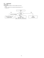
Page 22: ...First check point There are following 3 states of No Power indication by power LED 1 No lit 2 Green is lit then turns red blinking a few seconds later See 7 2 3 Only red is lit 7 3 No Power 22 ...

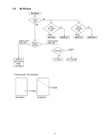
Page 23: ...7 4 No Picture 23 ...

Page 24: ...t P C B for each local area C6 board A D board A V C5 board A D board A V C4 board A D board л _ _ _ _ _ _ _ _ _ _ Y C3 board A D board _A _ Y C2 board A D board _A _ Panel Thin vertical line Local screen failure chart Y C1 board A D board SD board SC board SS board SS2 board SS3 board A board D board Fig 1 24 ...

Page 25: ...d electrically Note The board will be damaged if all connector is not removed for example remove connector only for SU board and stay connecting with SD board The board will be damaged 2 Connect SC jig to connector SC50 at left bottom side of SC board 3 Turn on the TV Display Unit and confirm the power LED blinking LED blinking Possible cause of failure is in SC board No LED blinking Lighting or n...

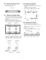
Page 26: ...e the P Board Caution To remove P C B wait 1 minute after power was off for dis charge from electrolysis capacitors 1 Unlock the cable clampers to free the cable 2 Disconnect the connectors P51 P52 P53 P54 and P55 P56 3 Disconnect the connectors P2 P6 P7 P9 P11 P25 P35 and P65 4 Remove the screws x9 O and remove the P MAIN Board 5 Remove the screws x6 and remove the P SUB Board 9 4 Remove the Side...

Page 27: ...unit 9 5 Remove the Tuner unit 9 6 Remove the A Board 1 Remove the Tuner unit See section 9 5 2 Remove the screws x3 and remove the A Board 1 Unlock the cable clampers to free the cable 2 Disconnect the Speaker terminal 3 Remove the screws x2 each and remove the Speak ers L R 9 7 Remove the Speakers 9 8 Remove the Woofer box 1 Unlock the cable clampers to free the cable 2 Disconnect the Relay conn...

Page 28: ... and SU5 connected to the SU Board 2 Remove the flexible cable SU11 SD11 and the bridge connector SC41 SU41 3 Remove the molding props x2 cz 4 Remove the screws x3 x2 and remove the SU Board 9 11 Remove the SD Board 1 Remove the flexible cables SD1 SD2 SD3 SD4 and SD5 connected to the SD Board 2 Remove the flexible cable SU11 SD11 and the bridge connectors SC42 SD42 and SC46 SD46 3 Remove the mold...

Page 29: ...Remove the screws x2 and remove the SS2 Board 1 Remove the Tuner unit See section 9 5 2 Disconnect the bridge connector SS03 SS22 and dis connect the flexible cables SS57 and SS59 3 Remove the screws x4 and remove the SS3 Board 9 14 Remove the SS3 Board 9 15 Remove the SS Board 1 Remove the Tuner unit See section 9 5 2 Unlock the cable clampers to free the cable 3 Disconnect the connector SS11 4 D...

Page 30: ...4 Remove the V bar connecting m etal bottoms L R fas tening screws x2 each and remove the V bar con necting metal bottoms L R and the Bracket covers L R 1 Remove the AC inlet See section 9 1 2 Disconnect the flexible cables D5 D20 D31 D32 D33 and D34 3 Disconnect the connectors D3 and D25 4 Remove the screws x4 and remove the D Board 9 18 Remove the D Board 9 19 Remove the C1 Board 1 Remove the Ha...

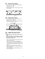
Page 31: ...e C4 Board 1 Remove the Hanger metal R See section 9 17 2 Remove the flexible cable holder fastening screws x 10 3 Disconnect the flexible cables CA1 CA2 CA3 CA4 and CA5 4 Disconnect the flexible cable C40 5 Remove the screws x5 and remove the C4 Board 9 23 Remove the C5 Board 1 Disconnect the flexible cable holder fastening screws x 1 0 O 2 Disconnect the flexible cables CA6 CA7 CA8 CA9 and CA10 ...

Page 32: ...move Side view 9 26 Remove the Contact metals 1 Remove the Cabinet assy See section 9 25 2 Remove the screws x2 3 Remove the Rear cover hooks L R Rear cover hook R Rear cover hook L Cabinet assy 4 Remove the screws хб O 5 Remove the Contact metal top 6 Remove the screws x 1 0 7 Remove the Contact metal bottom 8 Remove the screws x8 H 9 Remove the Contact metals L R Contact metal R Cabinet assy Con...

Page 33: ...w ithout Hanger metals is fragile To avoid the dam age to new plasm a panel carry a new plasm a panel taking hold o f the Hanger metals after assem bling the Hanger metals 1 Place a carton box packed a new plasma panel on the flat surface of the work bench 2 Open a box and without taking a new plasma panel Attach the C 1 C2 C3 C4 C5 and the C6 Board connect the flexible cables from the plasma pane...

Page 34: ...play will be displayed during TEST and CONF stage Press 5 button to display the On Screen Display Press VOL button to set to LOW In LO W setting a If no several dead pixel is visible remarkably in white pattern press 3 button to go to CONF stage b If the several dead pixels are visible rem arkably in white pattern Set to HIGH by press VOL button Press 3 button to go to CONF stage if the sym ptom i...

Page 35: ...Split Colour bar shown as below Note Sub contrast adjustment is unadjusted for AV HD input But when needing the adjustment cho sen manually please refer to alterna tive method 100 White 2 Goes into service mode 3 Push a 1 or 2 key and goes into service mode for CONTRAST Adjustment 1 The colour key yellow button of remote control is pushed 2 The OSD character of sub contrast becomes red Inside unde...

Page 36: ... Inside under automatic adjustment 3 The OSD character of sub contrast returns to black 4 End Steps Another procedure Adjustment of HD system 1 At 1080i 100 Full White or Split colour bar receive component signal as shown below Remarks 100 White 2 Goes into service mode 3 Push 1 or 2 key and goes into service mode for Contrast Adjustment 1 The colour key yellow button of remote control is pushed 2...

Page 37: ...ignal receiver of color analyzer to the INNER PATTERN s center and adjust B drive and R drive so x y become the COLOR TEMP COOL in the below table1 8 All RGB drive increase so that the maximum drive value of RGB may become FF ALL DRIVE set to FF 9 Set color balance to NORMAL using 7 key 10 Fix G CUTOFF B CUTOFF and R CUTOFF at 80 11 Set G DRIVE at D0 12 Adjust B DRIVE and R DRIVE so the INNER PATT...

Page 38: ...38 ...

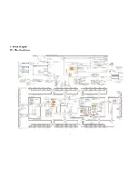
Page 39: ...11 Block Diagram 11 1 Main Block Diagram 39 ...

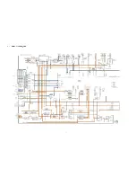
Page 40: ...11 2 Block 1 5 Diagram 40 ...

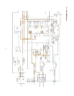
Page 41: ...Block 2 5 Diagram ...

Page 42: ...11 4 Block 3 5 Diagram г а P O W E R S U P P LY 42 ...

Page 43: ...______________________________________________________________________________________________________ __________________________________________________________________________________________________ ___________________ ___________________________________________________________________________________________________________ 1 43 ...

Page 44: ...11 6 Block 5 5 Diagram S C S C A N D R IV E 44 ...

Page 45: ......

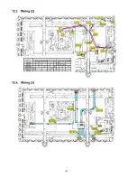
Page 46: ...gram 12 1 Caution statement Caution Please confirm that all flexible cables are assembled correctly Also make sure that they are locked in the connectors Verify by giving the flexible cables a very slight pull 12 2 Wiring 1 45 ...

Page 47: ...12 3 Wiring 2 46 ...

Page 48: ...12 5 Wiring 4 12 6 Wiring 5 47 ...

Page 49: ...12 7 Wiring 6 48 ...

Page 50: ...assis Earth Cold Line Earth Hot 6 Voltage Measurement Voltage is measured by a DC voltmeter Conditions of the measurement are the following Power Source AC220 240V 50 60Hz Receiving S ignal Colour Bar signal RF All customer s controls Maximum positions 7 When arrow mark is found connection is easily found from the direction of arrow 8 Indicates the major signal flow Video A u d io s 9 This schemat...

Page 51: ...ld Precautions a Do not touch the hot part or the hot and cold parts at the same time or you may be shocked b Do not short circuit the hot and cold circuits or a fuse may blow and parts may break c Do not connect an instrument such as an oscilloscope to the hot and cold circuits simultaneously or a fuse may blow Connect the earth of instruments to the earth connection of the circuit being measured...

Page 52: ...13 2 P MAIN Board 1 3 Schematic Diagram 50 ...

Page 53: ...13 3 P MAIN Board 2 3 Schematic Diagram A B C D E F i 2 3 4 5 6 7 51 ...

Page 54: ...PZDC221 I POW ER MICOM A О 1 5 Vo 2 O 2 1 5 V c 2 0 3 GND о GND о S T B Y 5 V О б GND о S0 о S I о P A M E L M a i n _ 0 N О 1 0S 0 S 4 _ P S О з о о О 1 0 S T B Y 5 V GND O i F _ S T B Y _ 0 N E C O O N S T B Y 5 V _ 0 N SO S4 _ PS A C _ L 0W ALI__O FF M A I N _ S W _ 1 NC M AI N _ S W _ 2 M AI N _ SW _ 1 NC M A IN _ S W _ 2 P M AIN BO ARD ETX2M M 813M DM 3 3 0 0 0 9 TO P SUB BOARD P55 TO P25 D B...

Page 55: ...13 5 P SUB Board Schematic Diagram 53 ...

Page 56: ...ree S A T FE D V B T 2 FE H K D FE C hina D FE B razil D FE j j n IC8601 Peaks EEP 32kE U R O 16kA SIA II IC 1100 G enX8 TO 14 25 1 TO 21 25 D A 0 t O 21 25 25 _ S s C d A TO 14 21 25 00 Vi IC 1101 G e n X EEP 8k IC TO 22 25 IC 8001 A VC 31 TO 14 25 25 TO 7 25 IC8301 C 3001 T E M P S E N S O R M M 3285A N R E FE C X D 19 78 R A T U N E R JTAG F 1 2 8 9 54 ...

Page 57: ...13 7 A Board 2 25 Schematic Diagram A A BOARD 2 25 Peaks DEST 55 ...

Page 58: ...13 8 A Board 3 25 Schematic Diagram A A BOARD 3 25 C om m and Inteface Buffers Level shifter IC Peaks DEST 19 20 21 22 23 24 25 2 6 2 7 TO 22 25 TO 22 25 56 ...

Page 59: ...OCK GEN H 0 J27 05 00 12 0 r EJ f tHUHT L J_C 8 П R 8 6 4 9 Г X E A S TO 3 25 PE A K S L D A 2 TO 22 25 LD ft27 4 17 58 24 M H z 1 J D E V IC E CLK P E A K S L D A 2 C 8150 R g PE A K S L D A 2 A chi8 X 8 0 0 2 В Д p H 0 J2 4 5 5 0 0 1 0 1 TO 22 25 j 8 2 4 5M H z J 0 JH C 0 0 0 4 5 57 ...

Page 60: ...13 10 A Board 5 25 Schematic Diagram A A BOARD 5 25 U SB ETH ERN ET U S B l F TO 4 25 E TH E R 2S M O 3 7 38 39 4 0 ...

Page 61: ...41 4 2 4 3 4 4 4 5 58 ...

Page 62: ...13 11 A Board 6 25 Schematic Diagram A A BOARD 6 25 CI SLOT SD CARD FLASH M EM O RY CI C O N N E C T O R TO 3 25 IC8950 TVRR874 Ie e p r o m 4 6 4 7 48 49 50 51 52 53 54 59 ...

Page 63: ...A A BOARD 7 25 GenX8 13 12 A Board 7 25 Schematic Diagram 5 5 5 6 5 7 5 8 5 9 60 ...

Page 64: ...60 61 62 6 3 ...

Page 65: ...13 13 A Board 8 25 Schematic Diagram A A BOARD 8 25 HDMI 6 4 1 6 5 1 6 6 1 6 7 1 6 8 1 6 9 1 7 0 1 71 1 72 61 ...

Page 66: ...13 14 A Board 9 25 Schematic Diagram A A BOARD 9 25 AD Buffer Q O t o 8 25 Euro O N L Y 7 3 74 75 76 7 7 62 ...

Page 67: ...Peaks Com mon 7 8 79 8 0 81 ...

Page 68: ...13 15 A Board 10 25 Schematic Diagram A A BOARD 10 25 AUDIO AMP P e ak s C O M M O N 82 8 3 8 4 85 ...

Page 69: ...86 8 7 88 89 9 0 63 ...

Page 70: ...13 16 A Board 11 25 Schematic Diagram A A BOARD 11 25 TERM INAL J K 3 0 0 1 K1 FY315A0008 PC IN D 3 0 1 5 K7AAAY000006 OPTICAL AUDIO OUT 91 92 93 94 ...

Page 71: ...EURO model A V S T M O D E L T 0 12 25 J K 3 0 0 2 K1 FY242A0001 JK31 00A К2 HA710A0001 9 5 1 9 6 1 9 7 1 9 8 1 9 9 64 ...

Page 72: ... N D A U D IO _4P _T EI A U D IO O U T M O N IT O R O U T _M J0 JY C 0 00 03 31 i j Q 1 0V1 0 u 330 1 0V1 0 u П Г 10V1 0 u j Г Н I J AV 1 I h V V 0 1 A A V S W C O M M O N IC3001 E_AV1 E _ A V 1 _V O IU T 1 9P A _V O U T _T E I E _ A V 2 _ V O IU T 1 9 P _ T E I in 3 V ID E O D ET T U N E R TO 13 25 IC 3001 TO 13 25 10 0 101 1 0 2 10 3 1 0 4 10 5 1 0 6 1 0 7 10 8 A U D IO O S G Q L IN K 1 Q3002 B ...

Page 73: ...13 18 A Board 13 25 Schematic Diagram A A BOARD 13 25 AV SW TO 12 25 AV1 V IN A V 3 V IN AV1 R G B YC 109 1 1 0 111 1 1 2 1 1 3 1 1 4 1 1 5 11 6 11 7 TO 12 25 YP b P r IN PC 66 ...

Page 74: ...13 19 A Board 14 25 Schematic Diagram A A BOARD 14 25 TU NE R STB R E SET A C T IV E A N T E N N A A _ D E T TO 7 25 R E S E T _ P O W E R _ D E T 118 119 120 121 122 123 124 125 126 67 ...

Page 75: ...13 20 A Board 15 25 Schematic Diagram A A BOARD 15 25 LVDS M O DEL TO D BOARD D5 127 128 129 13 0 ...

Page 76: ...131 1 3 2 1 3 3 1 3 4 13 5 68 ...

Page 77: ...13 21 A Board 16 25 Schematic Diagram A A BOARD 16 25 FRCS 13 6 1 3 7 1 3 8 13 9 1 4 0 141 1 4 2 1 4 3 14 4 69 ...

Page 78: ...13 22 A Board 17 25 Schematic Diagram A A BOARD 17 25 FRCS 1 4 5 1 1 4 6 1 1 4 7 1 1 4 8 1 1 4 9 1 1 5 0 1 151 1 1 5 2 1 1 5 3 70 ...

Page 79: ...gram A A BOARD 18 25 M IHO2 3D A f t TO 16 20 23 25 IC5806 C0DBAYY00605 У у д а Ц W L D A 2 M IH O 2 TO 22 25 IC5800 C1AB00003253 M IH O 2 F R C M IH O 2 l ED_5V_2 I LED D R IV E C IR C U IT 15 4 1 5 5 1 5 6 15 7 1 5 8 15 9 1 6 0 161 16 2 TO 17 71 ...

Page 80: ... l 1 О со I C M 0 1 L O C N I 0 5 Q a 0 C D 1 t f p p t i t Ь p p i f f p p t t t t t p p p E E E E E E E E E E E E E E E E E E E E E E E E E E E E E E E E E E E E E E E E E E E E E E E E i i i i i i i i i i i i I I I I I I I I I I I I S S S S S S S S S S S S 5 5 5 5 5 5 5 5 5 5 5 5 I1 1 1 1 1 1 1 1 1 1 1 1 1 1 1 1 1 1 1 1 1 1 1i i i i i i i i i i i i ШШШШ ШШ 11111119 1 1 1 1 1 1 1 1 1 1 iiiiiiiii...

Page 81: ...13 25 A Board 20 25 Schematic Diagram A A BOARD 20 25 POW ER Peaks IC5290 C0DBGYY00884 17 2 1 7 3 1 7 4 17 5 1 7 6 17 7 1 7 8 1 7 9 18 0 73 ...

Page 82: ...X TO 7 25 FAN TO P BOARD P6 TEMP SENSORl SW 2500 K0F122A00031 POWER SW Н Ц з П j i n 5 in __о Г 3 i П П Г S i in _n Г S i in ПI 3 2п__n Г П П П n n m И G Z Q D G en X L O C K P E A K S LD A 2 181 182 183 184 18 186 187 188 189 KEY TO 7 25 TO 7 25 TO 22 25 74 ...

Page 83: ... D V D D A V A D A V D D S IF C 1 0 A V D D P LLA E 8 A V D D 75D E 6 A V D D P LLV E 7 _V D D P U S B G 29 P 8Q Q l H 29 f 8Q Q l J29 С 8 00 K 29 с 8 00 L29 С 8 00 EtherP H Y H S 0P S Y N C H S 0V A L H S B C LK O U T H S S Y N C O U T H S V A L O U T H S D O U T 0 H S D O U T 1 H S D O U T 2 H S D O U T 3 H S D O U T 4 H S D O U T 5 H S D O U T 6 H S D O U T 7 H S B C LK O U T H S S Y N C O U T ...

Page 84: ...у ffi у ffi у Г т Г Т Г у Г Т Г у Г у Г Т Г у г т г т г т г т г т г т у й у й у Е у у Е у Г у у Г у Е у y E y i y y у Е у Г у m r I L 1 PDJ DDPLLSJ у Л у Л у Л у Л у Л у са pd_d ddi т о 4 22 25 у к у О pd Т о 22 25 X I X P E A K S L D A 2 A chip t T т у у т у Т у Г у з л л и з г Г у У у У у Г у У у А т m 1 m 1 1 f Л Л m m r т г г 7 19 9 2 0 0 201 2 0 2 2 0 3 76 ...

Page 85: ...IC 5 5 0 0 C0DBAYY0071 5 2 0 4 2 0 5 2 0 6 2 0 7 ...

Page 86: ...13 29 A Board 24 25 Schematic Diagram A A BOARD 24 25 DDR3 2 0 8 2 0 9 2 1 0 211 2 1 2 2 1 3 2 1 4 2 1 5 2 1 6 77 ...

Page 87: ...13 30 A Board 25 25 Schematic Diagram A A BOARD 25 25 OFDM 2 1 7 2 1 8 2 1 9 2 2 0 221 2 2 2 2 2 3 2 2 4 2 2 5 78 ...

Page 88: ...13 31 D Board 1 5 Schematic Diagram в D A D BOARD TZTNP01 LCUE 1 5 DC DC C O N VE R TE R 1 2 3 4 ...

Page 89: ...5 1 6 1 7 1 8 1 9 79 ...

Page 90: ...13 32 D Board 2 5 Schematic Diagram 10 1 11 1 12 1 13 1 14 1 15 1 16 1 1 7 1 18 80 ...

Page 91: ...13 33 D Board 3 5 Schematic Diagram 19 1 2 0 1 21 1 2 2 1 2 3 1 2 4 1 2 5 1 2 6 1 2 7 81 ...

Page 92: ...13 34 D Board 4 5 Schematic Diagram 2 8 2 9 30 31 32 3 3 3 4 3 5 3 6 82 ...

Page 93: ...13 35 D Board 5 5 Schematic Diagram 37 38 3 9 4 0 41 4 2 4 3 4 4 4 5 83 ...

Page 94: ...13 36 C1 Board Schematic Diagram A B C D E A C1 BOARD TXNC11LPUJ C20 F 1 2 3 4 5 84 ...

Page 95: ...13 37 C2 Board 1 2 Schematic Diagram A B C D E F A C2 BOARD TXNC21LPUJ 1 2 C 20 TO C1 BOARD C10 1 2 3 4 5 85 ...

Page 96: ...13 38 C2 Board 2 2 Schematic Diagram A Z A 17 20 4 K 4C D 01 00 00 13 1 0 I 11 1 12 1 13 1 14 1 15 1 16 1 17 1 18 C2 BOARD TXNC21LPUJ 2 2 86 ...

Page 97: ...13 39 C3 Board 1 2 Schematic Diagram F 1 2 3 4 5 87 ...

Page 98: ...13 40 C3 Board 2 2 Schematic Diagram A 10 I 11 12 13 14 C3 BOARD TXNC31 LPUJ 2 2 88 ...

Page 99: ...15 16 17 18 ...

Page 100: ...13 41 C4 Board Schematic Diagram A B C D E A C4 BOARD TXNC41LPUJ C50 F 1 2 3 89 ...

Page 101: ...13 42 C5 Board 1 2 Schematic Diagram A B C D A C5 BOARD TXNC51LPUJ 1 2 E C0JBAU000088 I BUFFER F 1 2 3 4 9 90 0 0 ...

Page 102: ...13 43 C5 Board 2 2 Schematic Diagram A C5 BOARD TXNC51LPUJ 2 2 10 i 1 1 1 12 1 13 1 14 1 1 5 1 16 1 17 1 18 91 ...

Page 103: ...13 44 C6 Board 1 2 Schematic Diagram A C6 BOARD TXNC61LPUJ 1 2 A 92 ...

Page 104: ...13 45 C6 Board 2 2 Schematic Diagram A C6 BOARD TXNC61 LPUJ 2 2 О fb C A 11 i 1 CA12 CA13 Л п I 1 In i 10 11 12 13 14 93 ...

Page 105: ...ь fbtq CA14 1 ь I CA15 я 15 16 17 18 ...

Page 106: ...13 46 SC Board 1 4 Schematic Diagram A B C D E A SC BOARD TXNSC1LPUJ 1 4 TO P BOARD P2 t p v s u s TO D BOARD D20 IC16561 F 3 4 5 94 ...

Page 107: ...13 47 SC Board 2 4 Schematic Diagram 10 I 11 1 12 1 13 1 14 1 1 5 1 16 1 17 1 18 95 ...

Page 108: ...13 48 SC Board 3 4 Schematic Diagram 19 1 2 0 1 21 1 2 2 1 2 3 1 2 4 1 2 5 1 2 6 1 2 7 96 ...

Page 109: ...13 49 SC Board 4 4 Schematic Diagram 2 8 2 9 3 0 31 3 2 3 3 3 4 3 5 3 6 97 ...

Page 110: ...13 50 A B C D E F SS Board 1 2 Schematic Diagram A SS BOARD TXN SS1LC U E 1 2 1 2 3 4 5 6 7 8 9 98 ...

Page 111: ...SS2 Board and SS3 Board Schematic Diagram SS24 SS02 SS22 SS03 A SS2 BOARD TNPA4983 PANEL SUSTAIN ELECTRODE IIII SS3 BOARD TNPA4984 PANEL SUSTAIN ELECTRODE hr PANEL SUSTAIN ELECTRODE 10 11 12 13 14 15 16 17 18 SS52 SS57 99 ...

Page 112: ...14 Printed Circuit Board 14 1 P MAIN Board P MAIN BOARD FOIL SIDE ETX2MM813MDM B G 6 5 4 3 2 1 E F H 100 ...

Page 113: ... 3 Q702 G 1 IC601 D 5 Q356 G 3 Q706 H 2 Q357 F 3 Q707 G 1 MODULE Q401 G 4 Q708 G 1 Q402 H 5 Q709 1 1 MC551 E 1 Q403 H 5 Q710 H 1 MC701 G 1 Q404 H 5 Q711 I 2 Q405 H 5 Q712 H 1 PHOTO COUPLER Q406 H 5 Q407 H 4 TEST POINT PC201 F 3 Q408 H 4 PC202 F 3 Q502 C 2 TP5 H 3 PC501 F 3 Q503 E 3 TP9 I 5 PC502 C 1 Q504 D 3 PC504 C 1 Q505 C 2 VOLUME PC510 D 1 Q506 C 1 VR251 H 3 Q507 D 1 VR401 H 5 Q508 D 1 Q551 F ...

Page 114: ...RD COMPONENT SIDE IC TRANSISTOR TEST POINT IC201 D 3 Q201 D 4 TP5 H 4 IC501 D 5 Q202 E 4 TP9 H 2 Q355 F 4 MODULE Q401 H 3 VOLUME Q402 H 2 MC551 E 6 Q403 H 2 VR251 H 4 MC701 G 6 Q551 F 4 VR401 H 2 Q601 D 2 Q604 E 2 Q606 E 2 101 ...

Page 115: ...P MAIN BOARD COMPONENT SIDE ETX2MM813MDM 6 5 4 3 2 1 A I B I C I D I E I F I G I H I I 102 ...

Page 116: ...01 D 2 TP5 H 1 IC901 E 3 Q802 D 2 IC902 D 4 Q803 D 2 IC951 H 3 Q804 E 2 VOLUME Q805 D 4 Q806 E 2 VR951 H 3 PHOTO COUPLER Q807 D 4 PC801 G 4 Q808 D 3 PC902 G 4 Q809 D 3 PC903 G 3 Q901 F 3 Q902 F 3 Q903 D 3 Q904 D 3 Q951 H 4 Q952 H 3 P SUB BOARD FOIL SIDE ETX2MM813MDS B G 6 5 4 3 2 1 E F H 103 ...

Page 117: ... Location P SUB BOARD COMPONENT SIDE IC TRANSISTOR TEST POINT IC901 E 2 Q801 D 3 TP5 H 3 Q804 E 3 Q806 E 3 Q901 F 2 VOLUME Q902 F 2 VR951 H 2 P SUB BOARD COMPONENT SIDE ETX2MM813MDS B G 6 5 4 3 2 1 E F H 104 ...

Page 118: ...14 3 6 5 4 3 2 1 K and V Board K BOARD FOIL SIDE TNPA5113AB V BOARD FOIL SIDE TXN V1LBUE K BOARD COMPONENT SIDE TNPA5113AB V BOARD COMPONENT SIDE TXN V1LBUE A I B I C I D I E I F I G I H I I 105 ...

Page 119: ...14 4 A Board A BOARD FOIL SIDE A PR65VT20 т а B G 6 5 4 3 2 1 E F H 106 ...

Page 120: ...A BOARD COMPONENT SIDE A PR65VT20 6 5 4 3 2 1 A I B I C I D I E I F I G I H I I 107 ...

Page 121: ...14 5 D Board 108 ...

Page 122: ...6 D BOARD COMPONENT SIDE TZTNP01LCUE A I В I С I D ...

Page 123: ......

Page 124: ...14 6 C1 Board C1 BOARD COMPONENT SIDE TXNC11LPUJ 1 A I B I C I D I E I F I G I H I I 110 ...

Page 125: ...14 7 C2 Board C2 BOARD FOIL SIDE TXNC21LPUJ C2 BOARD COMPONENT SIDE TXNC21LPUJ 6 5 4 3 2 1 A I B I C I D I E I F I G I H I I 111 ...

Page 126: ...14 8 C3 Board C3 BOARD FOIL SIDE TXNC31LPUJ 6 5 4 3 1 A I B I C I D I E I F I G I H I I 112 ...

Page 127: ...14 9 C4 Board 113 ...

Page 128: ...14 10 C5 Board 6 5 C5 BOARD FOIL SIDE TXNC51LPUJ 4 3 C5 BOARD COMPONENT SIDE TXNC51LPUJ 2 1 A I B I C I D I E I F I G I H I I 114 ...

Page 129: ...14 11 C6 Board 3 C6 BOARD COMPONENT SIDE TXNC61LPUJ 1 A I B I C I D I E I F I G I H I I 115 ...

Page 130: ...14 12 SC Board SC BOARD FOIL SIDE TXNSC1LPUJ В 116 ...

Page 131: ......

Page 132: ... SC BOARD COMPONENT SIDE TXNSC1LPUJ 6 5 4 3 2 1 A I B I C I D I E I F I G I H I I 117 ...

Page 133: ...14 13 SS Board 1 A I B I C I D I E I F I G I H I I 118 ...

Page 134: ...1 A I B I C I D I E I F I G I H I I 119 ...

Page 135: ... 1 Ц Ц ЦЦЦЦД a О IS S 0 2 9 SS3 BOARD FOIL SIDE TNPA4984 SS2 BOARD COMPONENT SIDE TNPA4983 i h a 9 8 H i 1 H CR 0 ISS02 j ISS2M M M A D 16446 K D I P I S S 5 2 ZA K d16444 i ф 0 i 1 1 3 SS3 BOARD COMPONENT SIDE TNPA4984 T N P A 4 9 8 4 M d SS3 DIP Л ф rf3f ISS57 lOo 6 5 4 3 2 1 A I B I C I D I E I F I G I H I I 120 ...

Page 136: ...15 Exploded View and Replacement Parts List 15 1 Exploded View and Mechanical Replacement Parts List 15 1 1 Exploded View 1 121 ...

Page 137: ...15 1 2 Exploded View 2 122 ...

Page 138: ...123 ...

Page 139: ...15 1 4 Packing 2 124 ...

Page 140: ...15 1 5 Mechanical Replacement Parts List Note All parts except parts mentioned PAVCCZ in the Remarks column are supplied byAVC CSPC Parts mentioned PAVCCZ are supplied by PAVCCZ 125 ...

Page 141: ...52Z SCREW BC TOP 4 12 chap 3 1 1 13 THEL074 SCREW 6 THTD020J SCREW A PRINT 4 4 THTF011N SCREW 83 14 TKKC5395 LED PANEL 1 15 TKKL54 93 M8 CAP 4 chap 3 1 5 16 TKKX5116 ALLEN WRENCH 1 17 TKPB45001B BRACKET COVER 2 18 TKXA2 5001 SP BOX FIXING BOSS HIGH 3 19 TMKG6 67 SPONGE FAN 3 20 TMKG8 96 SPONGE FAN CENTER 3 TMKY 997 SPACER 3 TMM2 3416 SPACER 1 TMM2 3417 CLAMPER 5 TMME2 85 CLAMPER 3 TMME2 87 EDGE SA...

Page 142: ...CZ 44 TPE0E9002 ACCESSORIES BAG 1 PAVCCZ 45 TPE0E9003 BAG FOR AC CORD 1 PAVCCZ 46 TPEB458 BAG PEDESTAL STAND 1 A 47 TQB0E2 02 99 INSTRUCTION BOOK KAZAKHSTAN 1 PAVCCZ 47 TQB0E2029L INSTRUCTION BOOK RUSSIAN 1 PAVCCZ A 47 TQB0E2029Y INSTRUCTION BOOK UKRAINIAN 1 PAVCCZ 49 TQEF098 BAG STAND ACCESSORY ASSY 1 50 TQEF118 BAG STAND POLE 1 51 TQEF119 BAG SCREW AND WRENCH 1 TQZJ10 9 SCREW USE MANUAL 1 61 TSX...

Page 143: ...BC 11 11 chap 3 1 2 XTV3 10JFJK SCREW REAR AV 2 2 XTV3 6GFJ SCREW 12 XTV3 8JFJ SCREW 4 XTWT4 Z15DFJ SCREW SP BOX 3 XYN3 F10FJK SCREW BC AC INLET 2 2 chap 3 1 4 XYN3 J10FJ SCREW 56 XYN4 E6FJ SCREW INLET 1 1 XYN4 F10FJ SCREW AL GHT 4 19 XYN4 F10FJ SCREW AL GHT 4 8 XYN4 F15FJK SCREW SPACER CAB 2 2 XYN5 F16FJ SCREW M5 16 4 XYN6 F14FJ SCREW HANGER METAL ASSY 10 10 88 XYN6 F25FJK SCREW 4 XZBT6506 POLY B...

Page 144: ...e of assembly and in accordance with the laws governing part and product retention After the end of this period the assembly will no longer be available Abbreviation of part name and description 1 Resistor 2 Capacitor Example Example ERD25TJ104 С ЮОКОНМ J 1 4W ECKF1H103ZF С 0 01UF Z 50V Type Allowance Type Allowance Type Allowance С Carbon F 1 F Fuse G 2 M Metal Oxide J 5 Metal Film К 10 S Solid M...

Page 145: ...6V 1 Safety Ref No Part No Part Name Description Pcs Remarks C2071 EEEHB0J101UR E 100UF 6 3V 1 C2072 EEEHB0J101UR E 100UF 6 3V 1 C2073 F1G1E333A091 C 0 033UF 25V 1 C2074 F1G1E333A091 C 0 033UF 25V 1 C2075 F1G1C104A116 C 0 1UF 16V 1 C2076 F1G1C104A116 C 0 1UF 16V 1 C2077 F1G1C104A116 C 0 1UF 16V 1 C2078 F1G1A105A047 C 1UF 10V 1 C2079 F1G1C103A116 C 0 01UF 16V 1 C2104 F1G1H100A731 C 10PF 50V 1 C2107...

Page 146: ...105K C 1UF 10V 1 C3047 ECJ1VB1A105K C 1UF 10V 1 C3048 ECJ1VB1A105K C 1UF 10V 1 C3049 ECJ1VB1A105K C 1UF 10V 1 Safety Ref No Part No Part Name Description Pcs Remarks C3064 F1G1H102A730 C 1000PF 50V 1 C3065 F1G1H102A730 C 1000PF 50V 1 C3070 F1J1A106A087 C 10UF 10V 1 C3071 F1J1A106A087 C 10UF 10V 1 C3072 F1G1C104A116 C 0 1UF 16V 1 C3073 F1J1A106A087 C 10UF 10V 1 C3078 F1J1A106A087 C 10UF 10V 1 C3083...

Page 147: ...16V 1 C4338 F1G1C104A116 C 0 1UF 16V 1 C4339 F1G1C104A116 C 0 1UF 16V 1 C4340 F1G1C104A116 C 0 1UF 16V 1 Safety Ref No Part No Part Name Description Pcs Remarks C4348 F1G1H101A731 C 100PF 50V 1 C4546 ECJ1VB0J105K C 1UF 6 3V 1 C4548 ECJ1VB0J105K C 1UF 6 3V 1 C4660 ECJ1VB0J105K C 1UF 6 3V 1 C4661 ECJ1VB0J105K C 1UF 6 3V 1 C4662 ECJ1VB0J105K C 1UF 6 3V 1 C4663 ECJ1VB0J105K C 1UF 6 3V 1 C4664 ECJ1VB0J...

Page 148: ... C5944 F1G1C104A116 C 0 1UF 16V 1 C5945 F1G1C104A116 C 0 1UF 16V 1 C5946 F1G1C104A116 C 0 1UF 16V 1 Safety Ref No Part No Part Name Description Pcs Remarks C5947 F1G1H102A730 C 1000PF 50V 1 C5948 F1G1C104A116 C 0 1UF 16V 1 C5949 F1G1H102A730 C 1000PF 50V 1 C5950 F1G1C104A116 C 0 1UF 16V 1 C5951 F1G1C104A116 C 0 1UF 16V 1 C5952 F1G1C104A116 C 0 1UF 16V 1 C5953 F1G1C104A116 C 0 1UF 16V 1 C5954 F1G1C...

Page 149: ...V 1 C8101 F1J1A106A087 C 10UF 10V 1 C8102 F1J1A106A087 C 10UF 10V 1 C8103 F1J1A106A087 C 10UF 10V 1 Safety Ref No Part No Part Name Description Pcs Remarks C8104 F1J1A106A087 C 10UF 10V 1 C8105 F1J1A106A087 C 10UF 10V 1 C8106 F1H0J475A041 C 4 7UF 16V 1 C8107 F1H0J475A041 C 4 7UF 16V 1 C8109 F1G1C104A116 C 0 1UF 16V 1 C8110 F1G1C104A116 C 0 1UF 16V 1 C8111 F1G1C104A116 C 0 1UF 16V 1 C8112 F1G1C104A...

Page 150: ...G1C104A116 C 0 1UF 16V 1 C8515 F1J1A106A087 C 10UF 10V 1 C8516 F1G1C103A116 C 0 01UF 16V 1 Safety Ref No Part No Part Name Description Pcs Remarks C8600 F1G1H102A730 C 1000PF 50V 1 C8711 F1J1A106A087 C 10UF 10V 1 C8712 F1G1C104A116 C 0 1UF 16V 1 C8713 F1G1C104A116 C 0 1UF 16V 1 C8714 F1G1H101A731 C 100PF 50V 1 C8717 F1J1A106A087 C 10UF 10V 1 C8718 F1G1C104A116 C 0 1UF 16V 1 C8719 F1G1C104A116 C 0 ...

Page 151: ...C9325 F1G1C104A116 C 0 1UF 16V 1 C9327 F1G1C104A116 C 0 1UF 16V 1 C9335 F1J1A106A087 C 10UF 10V 1 C9336 F1J1A106A087 C 10UF 10V 1 C9337 F1J1A106A087 C 10UF 10V 1 Safety Ref No Part No Part Name Description Pcs Remarks C9339 F1G1C104A116 C 0 1UF 16V 1 C9340 F1G1C104A116 C 0 1UF 16V 1 C9342 F1G1C104A116 C 0 1UF 16V 1 C9344 F1G1C104A116 C 0 1UF 16V 1 C9347 ECJ1VB0J105K C 1UF 6 3V 1 C9349 F1J1A106A087...

Page 152: ...401 C1AB00003230 IC 1 IC2780 C0ZBZ0001361 IC 1 IC2801 C0DBAYY00462 IC 1 IC2950 C0CBCAG00031 IC 1 IC2952 C0DBGYY00281 IC 1 IC3001 C1AB00003218 IC 1 Safety Ref No Part No Part Name Description Pcs Remarks IC4200 C1AB00003310 IC 1 IC4201 C0DBAYY00737 IC 1 IC4204 C0DBGFF00004 IC 1 IC4205 TVRR945 IC 1 PAVCCZ IC4206 C0DBGYY00892 IC 1 IC4207 C0DBGFF00011 IC 1 IC4211 C3ABSG000060 IC 1 IC4212 C0DBAYY00462 ...

Page 153: ...DUCTOR 1 L4701 J0JYC0000068 CHIP INDUCTOR 1 Safety Ref No Part No Part Name Description Pcs Remarks L4702 J0JYC0000068 CHIP INDUCTOR 1 L4703 J0JYC0000068 CHIP INDUCTOR 1 L4704 J0JYC0000068 CHIP INDUCTOR 1 L4705 J0JYC0000068 CHIP INDUCTOR 1 L4706 J0JYC0000068 CHIP INDUCTOR 1 L4707 J0JYC0000068 CHIP INDUCTOR 1 L4708 J0JYC0000068 CHIP INDUCTOR 1 L4712 J0JHC0000045 CHIP INDUCTOR 1 L4715 J0JYC0000068 C...

Page 154: ...1 Q5432 DSC2001S0L TRANSISTOR 1 Q5435 DSA200100L TRANSISTOR 1 Q5436 DSC200100L TRANSISTOR 1 Q5475 DSC2001S0L TRANSISTOR 1 Q5478 DSC200100L TRANSISTOR 1 Q5500 B1MBDDA00003 FET 1 Q5501 B1CFRD000048 FET 1 Q5502 B1MBDDA00003 FET 1 Q5503 B1MBEDA00015 FET 1 Q5504 B1CFRD000048 FET 1 Q5602 DSC2001S0L TRANSISTOR 1 Q5603 DSC2001S0L TRANSISTOR 1 Q5813 B1CFND000005 FET 1 Q5814 B1CFND000005 FET 1 Safety Ref No...

Page 155: ...Part No Part Name Description Pcs Remarks R2258 D0GA101JA015 M 100 OHM J 1 16W 1 R2259 D0GA101JA015 M 100 OHM J 1 16W 1 R2260 ERJ2GEJ103 M 10KOHM J 1 16 W 1 R2263 ERJ2GEJ103 M 10KOHM J 1 16 W 1 R2264 D0GA101JA015 M 100 OHM J 1 16W 1 R2301 ERJ2GEJ103 M 10KOHM J 1 16 W 1 R2302 EXB28V220J M 22 OHM 1 32 W 1 R2306 D0GA473JA015 M 47KOHM J 1 16W 1 R2307 D0GA472JA015 M 4 7KOHM J 1 16W 1 R2308 ERJ2GEJ221 M...

Page 156: ... Name Description Pcs Remarks R3021 D0GA222JA015 M 2 2KOHM J 1 16W 1 R3024 ERJ2GEJ104 M100KOHM J 1 16 W 1 R3025 ERJ2GEJ104 M100KOHM J 1 16 W 1 R3028 D0GA331JA015 M 330 OHM J 1 16W 1 R3029 D0GA331JA015 M 330 OHM J 1 16W 1 R3030 D0GA101JA015 M 100 OHM J 1 16W 1 R3041 D0GA331JA015 M 330 OHM J 1 16W 1 R3042 D0GA331JA015 M 330 OHM J 1 16W 1 R3072 ERJ6ENF1500 M 150 OHM F 1 8W 1 R3073 ERJ6ENF1500 M 150 O...

Page 157: ...Z0001 M 0 OHM 1 16W 1 R4229 ERJ2GEJ102X M 1KOHM J 1 16 W 1 R4230 D0GBR00Z0002 M 0 OHM J 1 10W 1 R4234 D0GA473JA015 M 47KOHM J 1 16W 1 R4235 ERJ2GEJ103 M 10KOHM J 1 16 W 1 R4241 D0GA101JA015 M 100 OHM J 1 16W 1 R4242 D0GA101JA015 M 100 OHM J 1 16W 1 Safety Ref No Part No Part Name Description Pcs Remarks R4243 D0GA101JA015 M 100 OHM J 1 16W 1 R4244 D0GA101JA015 M 100 OHM J 1 16W 1 R4245 D0GA101JA01...

Page 158: ...OHM J 1 1 R4702 ERJ2GEJ103 M 10KOHM W J 1 16 1 R4703 D0GA330JA015 M 33 16W OHM J 1 1 R4704 D0GA4 73JA015 M 47KOHM 16W J 1 1 Safety Ref No Part No Part Name Description Pcs Remarks R4706 ERJ2GEJ103 M 10KOHM J 1 16 W 1 R4707 D0GA473JA015 M 47KOHM J 1 16W 1 R4708 ERJ2GEJ103 M 10KOHM J 1 16 W 1 R4709 ERJ2GEJ103 M 10KOHM J 1 16 W 1 R4710 D0GA473JA015 M 47KOHM J 1 16W 1 R4711 ERJ2GEJ102X M 1KOHM J 1 16 ...

Page 159: ... Pcs Remarks R5309 D1BB5601A055 M 5 6KOHM J 1 10W 1 R5312 D0GA150JA015 M 15 OHM J 1 16W 1 R5315 D0GB102JA041 M 1KOHM J 1 10W 1 R5412 D0GA273JA015 M 27K OHM J 1 16W 1 R5413 ERJ2GEJ104 M100KOHM J 1 16 W 1 R5418 ERJ2GEJ104 M100KOHM J 1 16 W 1 R5419 D0GA683JA015 M 68KOHM J 1 16W 1 R5431 D0GA222JA015 M 2 2KOHM J 1 16W 1 R5432 D0GA332JA015 M 3 3KOHM J 1 16W 1 R5433 ERJ2GEJ102X M 1KOHM J 1 16 W 1 R5434 E...

Page 160: ...29 D0GA4 70JA015 M 47 OHM J 1 16W 1 R5830 D0GA4 70JA015 M 47 OHM J 1 16W 1 R5839 D0GA680JA015 M 68 OHM J 1 16W 1 R5840 ERJ2GEJ102X M 1KOHM J 1 16 W 1 R5841 D0GA680JA015 M 68 OHM J 1 16W 1 Safety Ref No Part No Part Name Description Pcs Remarks R5863 D0GA223JA015 M 22K OHM J 1 16W 1 R5864 D0GA223JA015 M 22K OHM J 1 16W 1 R5865 D0GA223JA015 M 22K OHM J 1 16W 1 R5868 D1BA2202A014 M 22KOHM J 1 16 W 1 ...

Page 161: ...GA561JA015 M 560OHM J 1 16W 1 R8326 D0GA472JA015 M 4 7KOHM J 1 16W 1 Safety Ref No Part No Part Name Description Pcs Remarks R8327 D0GA472JA015 M 4 7KOHM J 1 16W 1 R8381 D1BA75R0A014 M 75 OHM J 1 16 W 1 R8382 D1BA75R0A014 M 75 OHM J 1 16 W 1 R8383 D1BA75R0A014 M 75 OHM J 1 16 W 1 R8384 D1BA75R0A014 M 75 OHM J 1 16 W 1 R8393 ERJ2GEJ103 M 10KOHM J 1 16 W 1 R8394 ERJ2GEJ103 M 10KOHM J 1 16 W 1 R8395 ...

Page 162: ...68 OHM J 1 16W 1 R8491 D0GA680JA015 M 68 OHM J 1 16W 1 R8492 D0GA680JA015 M 68 OHM J 1 16W 1 Safety Ref No Part No Part Name Description Pcs Remarks R8493 D0GA680JA015 M 68 OHM J 1 16W 1 R8494 D0GA680JA015 M 68 OHM J 1 16W 1 R8495 D0GA680JA015 M 68 OHM J 1 16W 1 R8496 D0GA680JA015 M 68 OHM J 1 16W 1 R8497 D0GA680JA015 M 68 OHM J 1 16W 1 R8498 D0GA680JA015 M 68 OHM J 1 16W 1 R8499 D0GA680JA015 M 68...

Page 163: ...A015 M 2 7KOHM 16W J 1 1 R8743 ERJ2GEJ103 M 10KOHM W J 1 16 1 R8744 D1BA6201A014 M 6 2KOHM W J 1 16 1 Safety Ref No Part No Part Name Description Pcs Remarks R8745 D0GA472JA015 M 4 7KOHM J 1 16W 1 R8747 ERJ2GEJ103 M 10KOHM J 1 16 W 1 R8748 ERJ2GEJ103 M 10KOHM J 1 16 W 1 R8754 ERJ2GEJ103 M 10KOHM J 1 16 W 1 R8757 D1BA1600A014 M 160 OHM J 1 16 W 1 R8758 D1BA2402A014 M 24KOHM J 1 16 W 1 R8759 D1BA100...

Page 164: ...1 16 W 1 R9166 ERJ2GEJ103 M 10KOHM J 1 16 W 1 R9174 D0GB162JA041 M 1 6KOHM J 1 10W 1 Safety Ref No Part No Part Name Description Pcs Remarks R9175 D0GB162JA041 M 1 6KOHM J 1 10W 1 R9176 D0GB162JA041 M 1 6KOHM J 1 10W 1 R9177 D0GB162JA041 M 1 6KOHM J 1 10W 1 R9185 ERJ2GEJ220 M 22 OHM J 1 16 W 1 R9186 ERJ2GEJ220 M 22 OHM J 1 16 W 1 R9187 D0GA272JA015 M 2 7KOHM J 1 16W 1 R9188 D0GA272JA015 M 2 7KOHM ...

Page 165: ... 16 W 1 R9614 EXB38V470J M 47 OHM 1 16 W 1 R9616 EXB38V470J M 47 OHM 1 16 W 1 Safety Ref No Part No Part Name Description Pcs Remarks R9868 ERJ2GEJ104 M100KOHM J 1 16 W 1 R9871 ERJ2GEJ103 M 10KOHM J 1 16 W 1 R9880 ERJ2GEJ103 M 10KOHM J 1 16 W 1 R9881 ERJ2GEJ103 M 10KOHM J 1 16 W 1 R9882 ERJ2GEJ103 M 10KOHM J 1 16 W 1 R9884 ERJ2GEJ103 M 10KOHM J 1 16 W 1 R9900 D0GAR00Z0001 M 0 OHM 1 16W 1 R9901 D0G...

Page 166: ... 1 C16481 F1L2J1020001 C 1000PF 630V 1 C16490 F1H1C105A145 C 1 uF 16 V 1 C16491 F1L2J1020001 C 1000PF 630V 1 Safety Ref No Part No Part Name Description Pcs Remarks C16501 F1K1E105A029 C 1UF 25V 1 C16502 F1K1E475A134 C 4 7UF 25V 1 C16503 F2A1E471A102 E 470UF 25V 1 C16504 F1K1E475A134 C 4 7UF 25V 1 C16505 F1K1E105A029 C 1UF 25V 1 C16507 F1E2J221A002 C 220PF 630V 1 C16508 F1E2J221A002 C 220PF 630V 1...

Page 167: ...1A971 C 100PF 50V 1 C17602 F1H1C104A143 C 0 1UF 16V 1 C17603 F1H1H101A971 C 100PF 50V 1 C17608 ECJ1VB1A105K C 1UF 10V 1 C17610 F1L2A334A034 C 0 33 UF 200 V 1 C17612 ECJ1VB1A105K C 1UF 10V 1 C17613 F1L2A334A034 C 0 33 UF 200 V 1 C17616 ECJ1VB1A105K C 1UF 10V 1 Safety Ref No Part No Part Name Description Pcs Remarks C17617 F1L2A334A034 C 0 33 UF 200 V 1 C17620 ECJ1VB1A105K C 1UF 10V 1 C17622 F1L2A33...

Page 168: ...NER DIODE 1 D16822 B0ADCJ000100 DIODE 1 D16824 DZ2J330M0L ZENER DIODE 1 D16825 DZ2J330M0L ZENER DIODE 1 D16859 B0HCKS000002 DIODE 1 D16871 DZ2J240M0L ZENER DIODE 1 Safety Ref No Part No Part Name Description Pcs Remarks D16874 DZ2J051M0L ZENER DIODE 1 D16875 B0ACCJ000048 DIODE 1 D16893 DZ2J056H0L ZENER DIODE 1 D16901 B0ADCJ000100 DIODE 1 D16902 B0ACCJ000048 DIODE 1 D16920 B0ADCJ000100 DIODE 1 IC16...

Page 169: ...Q16885 B1BBCF000028 TRANSISTOR 1 Q16920 B1ABCN000007 TRANSISTOR 1 Q16921 B1ABCN000007 TRANSISTOR 1 Q16930 DSC2001Q0L TRANSISTOR 1 Q16931 B1ABCN000007 TRANSISTOR 1 Q16932 DSC2001Q0L TRANSISTOR 1 Safety Ref No Part No Part Name Description Pcs Remarks R16001 D0GF7R5JA047 M 7 5 OHM J 1 3W 1 R16002 D0GF7R5JA047 M 7 5 OHM J 1 3W 1 R16003 D0GF7R5JA047 M 7 5 OHM J 1 3W 1 R16004 D0GF7R5JA047 M 7 5 OHM J 1...

Page 170: ...27KOHM F 1 8W 1 R16466 ERJ6ENF5602 M 56KOHM F 1 8W 1 R16467 ERJ6ENF8202 M 82KOHM F 1 8W 1 R16468 ERJ6ENF8202 M 82KOHM F 1 8W 1 R16471 D0GB392JA041 M 3 9KOHM J 1 10W 1 R16472 D0GB222JA041 M 2 2KOHM J 1 10W 1 R16473 ERJ6GEYF561 M 560 OHM J 1 8W 1 R16474 D0GB102JA041 M 1KOHM J 1 10W 1 R16475 ERJ3GEYJ472 M 4 7KOHM J 1 10W 1 R16476 ERJ3GEYJ472 M 4 7KOHM J 1 10W 1 R16478 D0GB562JA041 M 5 6KOHM J 1 10W 1...

Page 171: ...59 M 10 OHM J 1 4W 1 Safety Ref No Part No Part Name Description Pcs Remarks R16684 ERJ6GEYJ221V M 220 OHM J 1 8W 1 R16685 ERJ6GEYJ221V M 220 OHM J 1 8W 1 R16686 D0GB103JA057 M 10K OHM J 1 10W 1 R16687 D1BB2702A055 M 27KOHM J 1 10W 1 R16688 D1BB8871A055 M8 87KOHM J 1 10W 1 R16690 ERJ3GEYJ472 M 4 7KOHM J 1 10W 1 R16691 ERJ8GEYJ563 M 56KOHM J 1 4W 1 R16692 ERJ6RBD152 M 1 5 kOHM D 1 10 W 1 R16694 ERJ...

Page 172: ...1 10W 1 R17109 ERJ3GEYJ101 M 100 OHM J 1 10W 1 R17110 ERJ3GEYJ101 M 100 OHM J 1 10W 1 Safety Ref No Part No Part Name Description Pcs Remarks R17111 D0GB201JA041 M 200 OHM J 1 10W 1 R17112 D0GB201JA041 M 200 OHM J 1 10W 1 R17113 D0GB201JA041 M 200 OHM J 1 10W 1 R17114 D0GB201JA041 M 200 OHM J 1 10W 1 R17115 ERJ3GEYJ101 M 100 OHM J 1 10W 1 R17116 D0GB102JA041 M 1KOHM J 1 10W 1 R17117 ERJ6GEYJ224 M ...

Page 173: ... S0S TH т мот t j w h o оог и TfrOYCTOzaooa frOS TH s s хеигец soa uoTq dT osaa 5 auieN З хеа ON ъх еа ON T MOT t j wh o оот и Т0ТГЛЯ9 ГНЯ 09LT d T мот t j wh o оот и Т0ТГЛЯ9 ГНЯ ZOSLTH T m 8 t j wh o hozz и гггляоэгня T0S TH T мг т г wh o т и ozoycohtzooq 8ZbLT d T мот т г ино оот и Т0ТГЛЯ9 ГНЯ LZbLTX T мот т г ино оот и Т0ТГЛЯ9 ГНЯ SZbLTX T мот т г ино оот и Т0ТГЛЯ9 ГНЯ SZbLTX T мг т г wh o т и ...

Page 174: ... AYRA3 62MSV7A ARRESTOR 1 д A602 AYRA3 62MSV7A ARRESTOR 1 C201 ECJ1VB1H332K C 3300PF 50V 1 C202 ACDE2R221KP 2kV 220p 1 C203 ACDE2R221KP 2kV 220p 1 Safety Ref No Part No Part Name Description Pcs Remarks C204 ECWH8473HA P 0 033UF 800V 1 C205 ECWH8473HA P 0 033UF 800V 1 Д C206 ACKX331KYP 250V 330p 1 C207 ECJ2XB1H104K C 0 1UF K 50V 1 C208 ACMBC681J5T 50V 680p 1 C209 ECJ1VC1H471J C 470PF J 50V 1 C211 ...

Page 175: ...VD1SS133T DIODE 1 D602 VD1SS133T DIODE 1 д D603 VDD15XB80 DIODE 1 D605 VD1SS133T DIODE 1 д D606 VD1N5406G 07 DIODE 1 Safety Ref No Part No Part Name Description Pcs Remarks D607 VDYG982C6R DIODE 1 D608 VDERA83 004T DIODE 1 D610 VD1SS133T DIODE 1 D701 VDERA83 004T DIODE 1 D705 VD1SS133T DIODE 1 D706 VD1SS133T DIODE 1 D707 VD1SS133T DIODE 1 D708 VD1SS133T DIODE 1 D709 VDRB721Q40 DIODE 1 Д F201 HU216...

Page 176: ...GB103JA057 M 10K OHM J 1 10W 1 R205 ERJ6GEYJ394 M 390KOHM J1 8W 1 R206 ERJ6GEYJ394 M 390KOHM J1 8W 1 R207 ERJ6GEYJ394 M 390KOHM J1 8W 1 R208 ERJ6GEYJ394 M 390KOHM J1 8W 1 R209 D0GB183JA057 M 18K OHM J 1 10W 1 R210 ERJ6RBD152 M 1 5KOHM D 1 10W 1 R211 ERJ3EKF1872 M18 7KOHM 1 10W 1 R213 ERX1SJ1R0 M 1 0 OHM J 1W 1 R214 ERX12SJ5R6J M 5 6 OHM J 1 2W 1 R215 ERG12SJ680J M 68 OHM J 1 2W 1 R216 ERG12SJ680J ...

Page 177: ...1 ERJ3GEYJ223 M 22KOHM J 1 10W 1 R522 ERJ6GEYJ180 M 18 OHM J 1 8W 1 R524 ERJ3GEYJ223 M 22KOHM J 1 10W 1 R525 ERJ6ENF1002 M 10KOHM F 1 8W 1 Safety Ref No Part No Part Name Description Pcs Remarks R526 ERJ3GEYJ472 M 4 7KOHM J 1 10W 1 R529 ARR5B100JC2 5W 10 OHM 1 R530 ERJ3GEYJ471 M 470 OHM J 1 10W 1 R531 ERJ6ENF1002 M 10KOHM F 1 8W 1 R532 ERJ6ENF4123 M 412KOHM F 1 8W 1 R533 ERJ6ENF4123 M 412KOHM F 1 ...

Page 178: ...7 M 10K OHM J 1 10W 1 R747 D0GB103JA057 M 10K OHM J 1 10W 1 R748 D0GB103JA057 M 10K OHM J 1 10W 1 R749 D0GB103JA057 M 10K OHM J 1 10W 1 Safety Ref No Part No Part Name Description Pcs Remarks R750 D0GB103JA057 M 10K OHM J 1 10W 1 R751 ERJ6GEYJ102V M 1K OHM J 1 8W 1 R752 D0GB103JA057 M 10K OHM J 1 10W 1 R755 ERJ6GEYJ472V M 4 7KOHM J 1 8W 1 R756 ERJ6GEYJ101V M 100 OHM J 1 8W 1 R757 ARRF5EJR15B 0 15 ...

Page 179: ... 1 IC951 VIJM1431AF IC 1 д K802 ALKQ3298M02 RELAY 1 Safety Ref No Part No Part Name Description Pcs Remarks Д K805 ALKQ3298M02 RELAY 1 Д L801 AYS251733HY FILTER CHOKE 1 Д L803 ETB42AZ14GAD TRANSFORMER 1 L901 AYTSKA170T FERRITE BEAD INDUCTOR 1 P2 AKB2P3S VH 2P CONNECTOR 1 Д P51 AKB2P4 VH B 2P CONNECTOR 1 Д P53 AKB2P VH 2P CONNECTOR 1 P55 AKB12B PH KS 12P CONNECTOR 1 Д PC801 VPS2581AL2HE OPTOISOLATO...

Page 180: ...0W 1 R935 ERJ3EKF1131 M1 13KOHM 1 10W 1 R936 ERDS2FJ472 C 4 7KOHM J 1 4W 1 R937 D0GB473JA057 M 47KOHM J 1 10W 1 R938 ERJ6RBD152 M 1 5KOHM D 1 10W 1 R939 ERDS2FJ103 C 10KOHM J 1 4W 1 R953 ERJ6GEY0R00V M 0 OHM 1 8W 1 R954 ERJ6GEYJ102V M 1K OHM J 1 8W 1 R956 ERJ6ENF3901 M 3 9KOHM F 1 8W 1 R957 ERJ6GEYJ472V M 4 7KOHM J 1 8W 1 R958 ERJ6GEYJ472V M 4 7KOHM J 1 8W 1 R959 ERJ6GEYJ472V M 4 7KOHM J 1 8W 1 R9...

Reviews: