1 Safety Precautions
1.1.
General Guidelines
6
1.2.
1. W h e n co n d u ctin g repairs and servicing, do not a tte m p t to m od ify th e equipm en t, its parts o r its m aterials.
2. W h e n w irin g units (w ith cables, fle xib le cab le s o r lead w ire s ) are sup plied as rep air parts and on ly one w ire o r som e o f th e
w ire s have been broken o r discon necte d, do not a tte m p t to rep air o r re-w ire th e units. R e pla ce th e en tire w irin g unit instead.
3. W h e n c on du cting repairs and servicing, do not tw is t the F asten co n n e cto rs but plug th e m stra ig h t in o r unplug th e m straig ht
out.
4. W h e n servicing, ob serve th e origin al lead dress. If a sh o rt circu it is found, replace all parts w h ich have been o ve rhe ated or
da m ag ed by the sh o rt circuit.
5. A fte r servicing, see to it th a t all th e pro te ctive de vice s such as in sulation barriers, in sula tion papers shield s are p ro pe rly
installed.
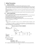
A fte r servicing, m ake th e fo llo w in g le akage c u rre n t che cks to p re ve n t th e c u s to m e r fro m being exposed to s h o c k hazards.
Touch-Current Check
1. Plug th e A C cord directly into th e A C outlet. Do not use an isolation tra n s fo rm e r fo r th is check.
2. C o n n e c t a m ea surin g n e tw o rk fo r to u ch curre nts betw een each exp ose d
m etallic part on th e set and a good earth ground
such as a w a te r pipe, as sho w n in F igure 1.
3. U se Le aka ge C u rre n t T ester (S im pson 228 o r e q u iv a le n t) to m ea sure th e po tential acro ss th e m ea surin g network.
4. C h e c k each exp ose d m etallic part, and m ea sure th e v o lta g e at each point.
5. R e serve th e A C plug in th e A C o u tle t and rep ea t each o f th e ab o ve m easure.
6. T he po tential at any po in t (T O U C H C U R R E N T ) e xp resse d as v o lta g e U
1
and U
2
, does not exce ed th e fo llo w in g values:
F or a. c.: U
1
= 35 V (pe ak) and U
2
= 0.35 V (peak);
F or d. c.: U 1 = 1.0 V,
Note:
T he lim it v a lu e o f U
2
= 0.35 V (pe ak) fo r a. c. and U
1
= 1.0 V fo r d. c. c orre spo nd to th e v a lu e s 0.7 m A (pe ak) a. c. and 2.0
m A d. c.
T he lim it va lu e U
1
= 35 V (pe ak) fo r a. c. corre spo nd to th e va lu e 70 m A (pe ak) a. c. fo r fre q u e n c ie s g re a te r tha n 100 kHz.
7. In case a m e a s u re m e n t is out o f the lim its specified, th e re is a po ssib ility o f a s h o c k hazard, and th e e q u ip m e n t should
be
repaired and rech ecke d be fore it is returned to th e custom er.
Measuring network for TOUCH CURRENTS
COLD
WATER PIPE
(EARTH GROUND)
Rs=
1500Q
_ L Cs=
0.22|
j
F
10kQ
-1
k
1
-------
1
Ro=
----------------
J
500Q
'
U
1
=
r
= 0.022|
j
F
( V )
JQ
LjJ JUUii
U
1
—|— и.и^гф Г
^ V
J
| U
2
(V)
APPLIANCES
EXPOSED
METAL PARTS
Resistance values in ohms (Q)
V:
Voltmeter or oscilloscope
(r.m.s. or peak reading)
Input resistance:
> 1 MQ
Input capacitance: < 200 pF
Frequency range: 15 Hz to 1 MHz and d.c. respectively
NOTE - Appropriate measures should be taken to obtain the correct value in case of non-sinusoidal waveforms.
Figure 1
3
Summary of Contents for TX-PR65VT20
Page 23: ...7 4 No Picture 23 ...
Page 38: ...38 ...
Page 39: ...11 Block Diagram 11 1 Main Block Diagram 39 ...
Page 40: ...11 2 Block 1 5 Diagram 40 ...
Page 41: ...Block 2 5 Diagram ...
Page 42: ...11 4 Block 3 5 Diagram г а P O W E R S U P P LY 42 ...
Page 44: ...11 6 Block 5 5 Diagram S C S C A N D R IV E 44 ...
Page 45: ......
Page 47: ...12 3 Wiring 2 46 ...
Page 48: ...12 5 Wiring 4 12 6 Wiring 5 47 ...
Page 49: ...12 7 Wiring 6 48 ...
Page 52: ...13 2 P MAIN Board 1 3 Schematic Diagram 50 ...
Page 53: ...13 3 P MAIN Board 2 3 Schematic Diagram A B C D E F i 2 3 4 5 6 7 51 ...
Page 55: ...13 5 P SUB Board Schematic Diagram 53 ...
Page 57: ...13 7 A Board 2 25 Schematic Diagram A A BOARD 2 25 Peaks DEST 55 ...
Page 61: ...41 4 2 4 3 4 4 4 5 58 ...
Page 63: ...A A BOARD 7 25 GenX8 13 12 A Board 7 25 Schematic Diagram 5 5 5 6 5 7 5 8 5 9 60 ...
Page 64: ...60 61 62 6 3 ...
Page 67: ...Peaks Com mon 7 8 79 8 0 81 ...
Page 69: ...86 8 7 88 89 9 0 63 ...
Page 76: ...131 1 3 2 1 3 3 1 3 4 13 5 68 ...
Page 85: ...IC 5 5 0 0 C0DBAYY0071 5 2 0 4 2 0 5 2 0 6 2 0 7 ...
Page 89: ...5 1 6 1 7 1 8 1 9 79 ...
Page 90: ...13 32 D Board 2 5 Schematic Diagram 10 1 11 1 12 1 13 1 14 1 15 1 16 1 1 7 1 18 80 ...
Page 91: ...13 33 D Board 3 5 Schematic Diagram 19 1 2 0 1 21 1 2 2 1 2 3 1 2 4 1 2 5 1 2 6 1 2 7 81 ...
Page 92: ...13 34 D Board 4 5 Schematic Diagram 2 8 2 9 30 31 32 3 3 3 4 3 5 3 6 82 ...
Page 93: ...13 35 D Board 5 5 Schematic Diagram 37 38 3 9 4 0 41 4 2 4 3 4 4 4 5 83 ...
Page 94: ...13 36 C1 Board Schematic Diagram A B C D E A C1 BOARD TXNC11LPUJ C20 F 1 2 3 4 5 84 ...
Page 97: ...13 39 C3 Board 1 2 Schematic Diagram F 1 2 3 4 5 87 ...
Page 98: ...13 40 C3 Board 2 2 Schematic Diagram A 10 I 11 12 13 14 C3 BOARD TXNC31 LPUJ 2 2 88 ...
Page 99: ...15 16 17 18 ...
Page 100: ...13 41 C4 Board Schematic Diagram A B C D E A C4 BOARD TXNC41LPUJ C50 F 1 2 3 89 ...
Page 103: ...13 44 C6 Board 1 2 Schematic Diagram A C6 BOARD TXNC61LPUJ 1 2 A 92 ...
Page 105: ...ь fbtq CA14 1 ь I CA15 я 15 16 17 18 ...
Page 107: ...13 47 SC Board 2 4 Schematic Diagram 10 I 11 1 12 1 13 1 14 1 1 5 1 16 1 17 1 18 95 ...
Page 108: ...13 48 SC Board 3 4 Schematic Diagram 19 1 2 0 1 21 1 2 2 1 2 3 1 2 4 1 2 5 1 2 6 1 2 7 96 ...
Page 109: ...13 49 SC Board 4 4 Schematic Diagram 2 8 2 9 3 0 31 3 2 3 3 3 4 3 5 3 6 97 ...
Page 115: ...P MAIN BOARD COMPONENT SIDE ETX2MM813MDM 6 5 4 3 2 1 A I B I C I D I E I F I G I H I I 102 ...
Page 119: ...14 4 A Board A BOARD FOIL SIDE A PR65VT20 т а B G 6 5 4 3 2 1 E F H 106 ...
Page 120: ...A BOARD COMPONENT SIDE A PR65VT20 6 5 4 3 2 1 A I B I C I D I E I F I G I H I I 107 ...
Page 121: ...14 5 D Board 108 ...
Page 122: ...6 D BOARD COMPONENT SIDE TZTNP01LCUE A I В I С I D ...
Page 123: ......
Page 124: ...14 6 C1 Board C1 BOARD COMPONENT SIDE TXNC11LPUJ 1 A I B I C I D I E I F I G I H I I 110 ...
Page 126: ...14 8 C3 Board C3 BOARD FOIL SIDE TXNC31LPUJ 6 5 4 3 1 A I B I C I D I E I F I G I H I I 112 ...
Page 127: ...14 9 C4 Board 113 ...
Page 129: ...14 11 C6 Board 3 C6 BOARD COMPONENT SIDE TXNC61LPUJ 1 A I B I C I D I E I F I G I H I I 115 ...
Page 130: ...14 12 SC Board SC BOARD FOIL SIDE TXNSC1LPUJ В 116 ...
Page 131: ......
Page 132: ... SC BOARD COMPONENT SIDE TXNSC1LPUJ 6 5 4 3 2 1 A I B I C I D I E I F I G I H I I 117 ...
Page 133: ...14 13 SS Board 1 A I B I C I D I E I F I G I H I I 118 ...
Page 134: ...1 A I B I C I D I E I F I G I H I I 119 ...
Page 137: ...15 1 2 Exploded View 2 122 ...
Page 138: ...123 ...
Page 139: ...15 1 4 Packing 2 124 ...

