


installed.
Caution
Be sure no power is applied to the chassis or circuit, and observe
all other safety precautions.
8. Minimize bodily motions when handling unpackaged replacement
ES devices. (Otherwise hamless motion such as the brushing
together of your clothes fabric or the lifting of your foot from a
carpeted floor can generate static electricity (ESD) sufficient to
damage an ES device).
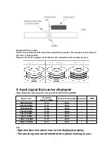
3. About lead free solder (PbF)
Note: Lead is listed as (Pb) in the periodic table of elements.In the information below, Pb will
refer to Lead solder, and PbF will refer to Lead Free Solder.The Lead Free Solder used in our
manufacturing process and discussed below is (Sn+Ag+Cu).That is Tin (Sn), Silver (Ag) and
Copper (Cu) although other types are available.
This model uses Pb Free solder in it.s manufacture due to environmental conservation issues.
For service and repair work, we.d suggest the use of Pb free solder as well, although Pb solder
may be used.
PCBs manufactured using lead free solder will have the PbF within a leaf Symbol
stamped on the back of PCB.
Caution
- Pb free solder has a higher melting point than standard solder.
Typically the melting point is 50 ~ 70°F (30~40°C) higher.
Please use a high temperature soldering iron and set it to 700 ±
20°F (370 ± 10°C).
- Free solder will tend to splash when heated too high (about 1100°F
or 600°C).
If you must use Pb solder, please completely remove all of the Pb
free solder on the pins or solder area before applying Pbsolder. If
this is not practical, be sure to heat the Pb free solder until it
melts, before applying Pb solder.
- After applying PbF solder to double layered boards, please check
the component side for excess solder which may flow onto the
opposite side. (see figure below)
6
Summary of Contents for TX-32LX60M
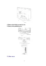
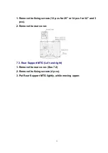
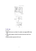
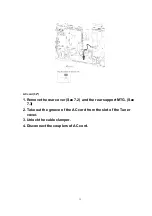
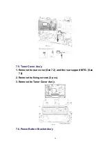
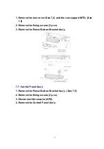
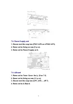
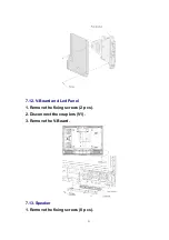
Page 10: ...4 Remove the fixing screws 4 pcs 5 Remove the pedestal ass y 7 2 Rear cover 10 ...
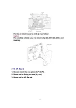
Page 24: ...8 Location of Lead Wiring Location of Lead Wiring 26 Location of Lead Wiring 32 24 ...
Page 25: ...9 EMI Processing EMI Processing 26 EMI Processing 32 25 ...
Page 27: ...10 3 Option Description 27 ...
Page 28: ...28 ...
Page 33: ...32 15 Packing Exploded View 26 33 ...
Page 34: ...32 34 ...
Page 36: ...17 2 Electrical Replacement Parts List 18 SCHEMATIC DIAGRAM FOR PRINTING WITH A4 36 ...